OLED displays fabricated by inkjet printing

An organic electronic device and a manufacturing method technology, applied in the field of OLED devices, can solve the problems of increasing processing time, increasing processing time, etc., to achieve the effect of improving processing time and avoiding processing problems

Active Publication Date: 2014-07-09
CAMBRIDGE DISPLAY TECH LTD
View PDF14 Cites 10 Cited by
  • Summary
  • Abstract
  • Description
  • Claims
  • Application Information

AI Technical Summary

Problems solved by technology

However, this triples the processing time and also starts to introduce uniformity issues as the first print starts to dry out in the printer cabinet in a relatively uncontrolled manner before the third and final print is done
Each of the three prints can be dried independently, but this further increases processing time

Method used


Image

  • OLED displays fabricated by inkjet printing
  • OLED displays fabricated by inkjet printing
  • OLED displays fabricated by inkjet printing

Examples


Embodiment Construction

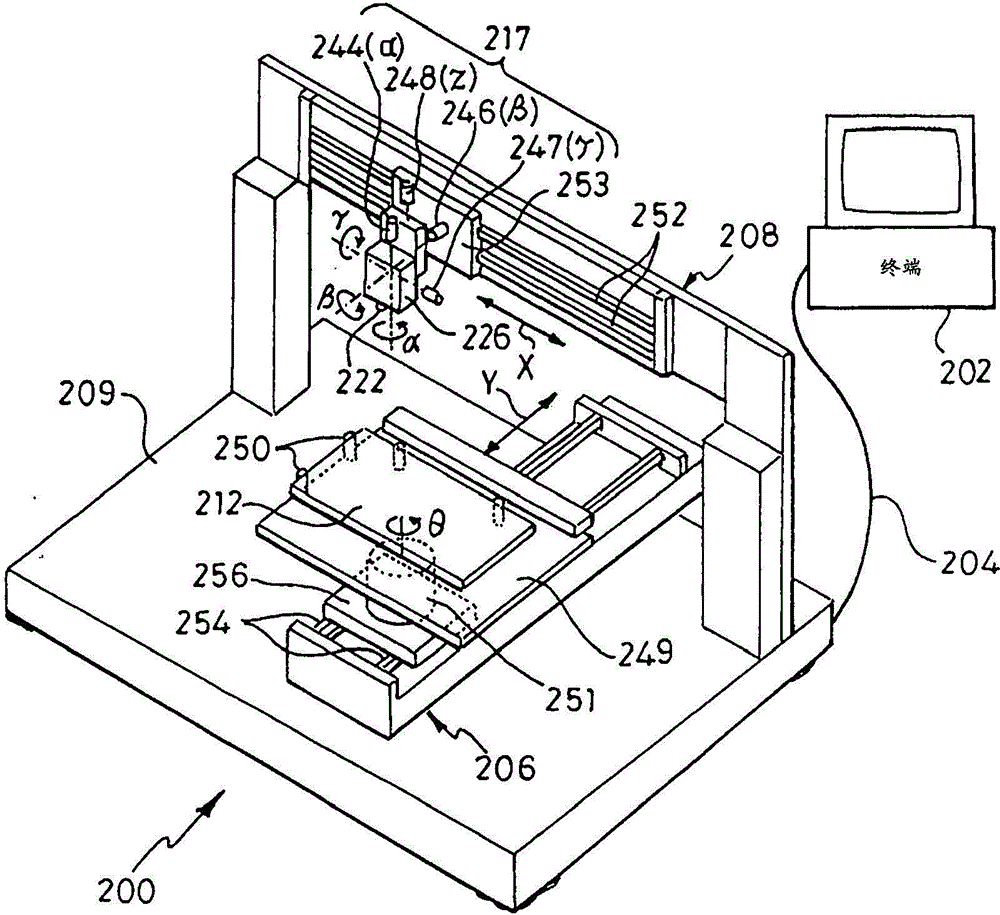
[0039] Examples of printers that we use for OLED fabrication are Litrex1408, Litrex142 and Litrex140P printers with Dimatix SX3 inkjet printheads (from Fujifilm Dimatix Inc.). Typically, the printhead prints successive swaths, say in the Y direction, stepping in the X direction between each swath. Optionally, the printhead can assume an angle Φ with respect to the X direction to reduce the dot pitch by a factor of cos Φ.

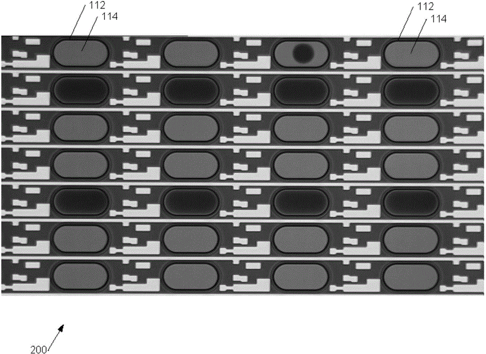
[0040] Figure 3a The passage of the scan head 222 over several pixels of a portion of a color OLED display is shown. The figure schematically represents the deposited droplets within a "polo" shaped annular bank 112 . In the figure, the red (R), green (G) and blue (B) sub-pixels respectively have separate wells based on the anode metal 14 . By way of example only, in a small flat panel display a pixel may have a width of 50 μm and a length of 150 μm to 250 μm, say a 10 μm or 20 μm wide bank; in a larger display more suitable for applications such as colo...


PUM

PropertyMeasurementUnit
thicknessaaaaaaaaaa
thicknessaaaaaaaaaa

Abstract

Provided is a method of fabricating an organic electric device, the method comprising: providing a substrate having at least two sets of material deposition regions, a first set of regions for a first set of elements of said device and a second set of regions for a second set of elements of said device, wherein said first and second sets of material deposition regions have different respective first and second target thickness of material to be deposited into said regions; providing at least one solution of material to be deposited on said first and second sets of regions; and ink jet printing said solutions of material onto said first and second sets of material deposition regions; wherein said ink jet printing comprises: depositing said at least one solution of material using a print head comprising a plurality of nozzles, a first subset of said nozzles is used for deposition onto said first set of regions and a second subset of said nozzles is used for deposition onto said second set of regions; and driving said first set of nozzles with a first drive waveform and said second set of nozzles with a second, different drive waveform for depositing said different respective first and second target thicknesses of material.

Description

technical field [0001] The present invention relates to techniques for fabricating organic electronic devices, in particular OLED devices such as polymer OLED (Organic Light Emitting Diode) displays. Background technique [0002] Figure 1a A cross-sectional view of a typical OLED device 10 is shown. It comprises a substrate 12 carrying a layer 14 of a transparent conductive oxide, typically ITO (Indium Tin Oxide). The transparent conductive oxide layer 14 can be patterned and typically has a thickness of about 40 nm. A hole injection layer (HIL) 16 typically comprising a conducting polymer such as PSS:PEDOT (polystyrene-sulfonate-doped polyethylene-dioxythiophene) is deposited thereon. This helps to match the hole energy levels of the ITO anode and light-emitting polymer (and can also help to planarize the ITO), which is typically about 30nm thick, but can reach about 150nm. Similar layers are generally present in organic photovoltaic devices to facilitate hole extractio...

Claims


Application Information

Patent Timeline
Patent Type & Authority Applications(China)
IPC IPC(8): H01L51/56B41M5/00
CPCH10K71/135Y02E10/549H10K50/852H10K59/30H10K99/00H10K10/00H10K71/00
Inventor J·爱萨克E·伯顿
Owner CAMBRIDGE DISPLAY TECH LTD
Why Eureka
Try Eureka