Drive circuit for GaN power devices

A technology for driving circuits and power devices, which is used in output power conversion devices, electrical components, and high-efficiency power electronic conversion. consumption, overcome the effect of overcharging

Inactive Publication Date: 2014-07-09
UNIV OF ELECTRONICS SCI & TECH OF CHINA
View PDF3 Cites 27 Cited by
  • Summary
  • Abstract
  • Description
  • Claims
  • Application Information

AI Technical Summary

Problems solved by technology

But there are also some factors that need special attention: low threshold voltage; upper gate-source voltage V GS(MAX) low; reverse conduction
[0004] The above-mentioned factors that need special consideration will cause some problems when driving GaN devices: low threshold voltage: there will be leakage inductance and gate capacitance on the gate drive path in the actual circuit, and these parasitic factors will cause oscillation during the switching transient, Some small voltage rises are usually detected by the gate, which eventually leads to false turn-on or even punch-through; the most commonly used gate drive circuit is a push-pull output structure, such as figure 1 As shown, using a P-type FET as the high side and an N-type FET as the low side
V F is the diode voltage drop, V DD Typically 5V, due to V sd_Q2 increases rapidly with increasing load current, making V boot The value of can quickly rise and even exceed the maximum voltage, causing damage to the gate of the high-side FET
Therefore, the current traditional drive circuits for MOS power devices are not suitable for GaN power devices

Method used


Image

  • Drive circuit for GaN power devices
  • Drive circuit for GaN power devices
  • Drive circuit for GaN power devices

Examples


Embodiment Construction

[0015] Below in conjunction with accompanying drawing, describe technical scheme of the present invention in detail:

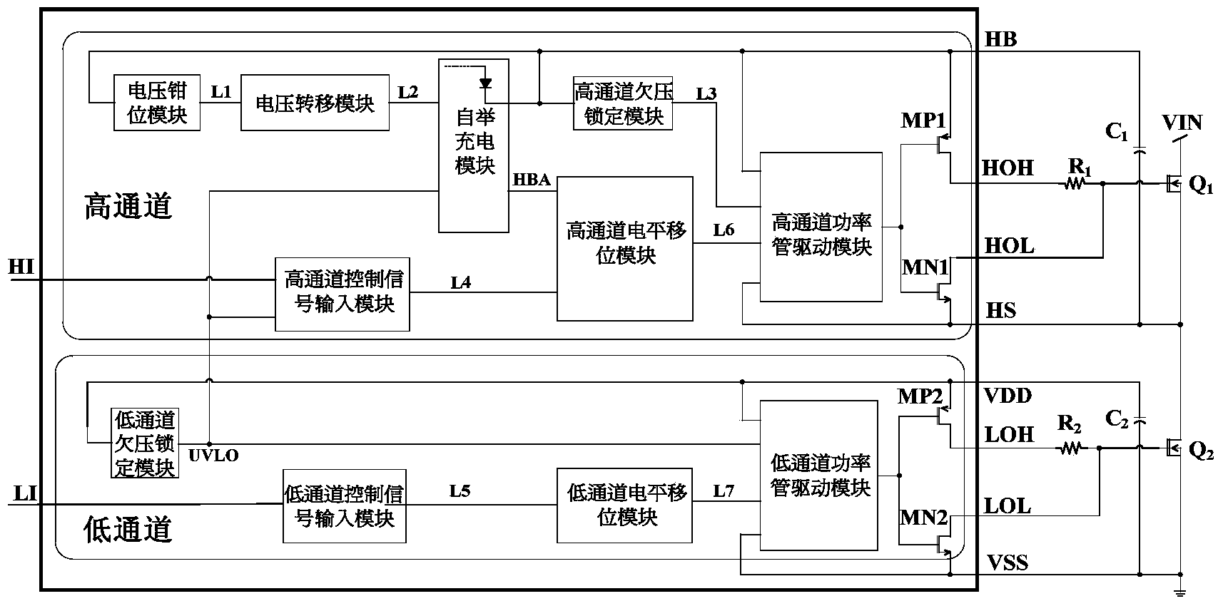
[0016] According to the characteristics of GaN FETs, based on the traditional half-bridge drive principle, the present invention proposes a fully integrated half-bridge drive circuit suitable for GaN FETs, the specific circuit structure is as follows image 3 As shown, including bootstrap capacitor voltage clamping module CLAMP, voltage transfer module LEVEL_DOWN, bootstrap charging module BOOT, high channel undervoltage lockout module UVLO_HS, high channel control signal input module HIN, high channel level shift module LEVEL_UPHS, high channel Power tube driver module DRIVER_HS, low-channel undervoltage lockout module UVLO, low-channel control signal input module LIN, low-channel level shift module LEVEL_UPLS, low-channel power tube driver module DRIVER_LS, PMOS tubes MP1, MP2, NMOS tubes MN1, MN2, GaN FET Q 1 , Q 2 , resistor R 1 , R 2 , capacitance C ...


PUM


Abstract

The invention relates to the technical field of integrated circuits, in particular to a drive circuit for GaN power devices. The drive circuit for the GaN power devices is characterized by comprising a high-channel drive module, a low-channel drive module, the GaN FET Q1 and the GaN FET Q2. High-channel power supply voltage HB and high-channel ground potential HS are adopted for the high-channel drive module, and the output end of the high-channel drive module is connected with the grid electrode of the GaN FET Q1. Power supply voltage VDD and ground potential VSS are adopted for the low-channel drive module, and the output end of the low-channel drive module is connected with the grid electrode of GaN FET Q2. The drain electrode of the GaN FET Q1 is connected with external voltage VIN, and the source electrode of the GaN FET Q1 is connected with the drain electrode of the GaN FET Q2. The drive circuit for the GaN power devices has the advantages that the situation that voltage across the two ends of a bootstrap capacitor exceeds the maximum limit gate-to-source voltage of the GaN FETs is effectively prevented, and the problems that as GaN FETs are not provided with body diodes, a bootstrap circuit is overcharged within dead time, and a high-end FET is prone to damage are solved. The drive circuit is especially applicable to the GaN power devices.

Description

technical field [0001] The invention relates to the technical field of integrated circuits, in particular to a driving circuit for GaN power devices. Background technique [0002] As the application market pays more and more attention to energy efficiency and the pursuit of high-performance and low-cost electronic products, the consideration of device and system efficiency, performance, and cost in the field of power electronics will run through the entire process of power semiconductors from research and development to production. There is no doubt that GaN devices and their power systems will meet the performance requirements of future power electronics for high power, low loss, high speed, and high reliability by virtue of their material characteristics. [0003] Compared with Si MOSFETs, GaN FETs mainly have the following characteristics: under the same withstand voltage, the on-resistance and device volume are small; the switching speed is fast; the current density is l...

Claims


Application Information

Patent Timeline
Patent Type & Authority Applications(China)
IPC IPC(8): H02M1/08
CPCY02B70/10
Inventor 周泽坤王霞吴刚石跃孙亚东明鑫王卓张波
Owner UNIV OF ELECTRONICS SCI & TECH OF CHINA
Why Eureka
Try Eureka