
Image sensor micro lens structure for improving sensitivity of red pixels and blue pixels
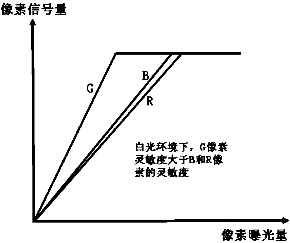
An image sensor and blue pixel technology, applied in the field of image sensors, can solve problems such as difficult image color correction operation, complicated signal white balance processing, and different photosensitivity, so as to achieve approximate photosensitivity, reduce processing complexity, and improve sensitivity Effect
- Summary
- Abstract
- Description
- Claims
- Application Information
AI Technical Summary
Problems solved by technology
Method used
Image

Examples
specific Embodiment approach
[0021] The image sensor microlens structure that improves red and blue pixel sensitivity of the present invention, its preferred embodiment is:
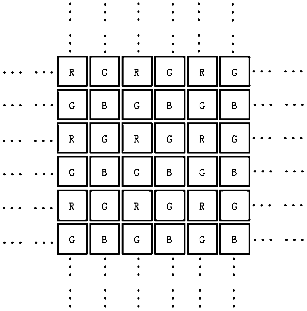
[0022] The pixel array of the image sensor adopts the red, green and blue arrangement of the Bayer pattern, and the microlens plane area of the red pixel and the blue pixel is larger than the microlens plane area of the green pixel.
[0023] The plane area of the microlens of the red pixel and the blue pixel is 1.2 to 1.3 times the plane area of the microlens of the green pixel.
[0024] The microlens plane areas of the red pixels and the blue pixels are equal or unequal.
[0025] The plane shapes of the microlenses of the red pixels, blue pixels and green pixels are polygons.
[0026] The plane shapes of the microlenses of the red pixels, blue pixels and green pixels are square or rectangular.
[0027] The image sensor micro-lens structure improving the sensitivity of red and blue pixels is used in a CMOS type image sensor...
specific Embodiment
[0029] In the embodiment, the pixel size of the RGB three colors is a square structure as an example, and the area of the R pixel and the B pixel are equal as an example.
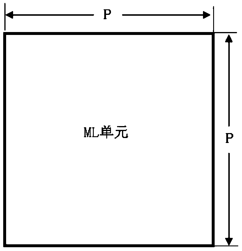
[0030] Figure 4a , 4b as shown, Figure 4a Schematic diagram of the plane size of the ML (microlens) unit used for the G pixel, the size of which is PgXPg; Figure 4b Schematic diagram of the ML unit plane size used for R and B pixels, the size of which is PrbXPrg, where the ML plane area of R and B pixels is 1.2 to 1.3 times the ML plane area of G pixel. Figure 4a , 4b The ML plane area used by the R and B pixels shown is larger than the ML plane area used by the G pixel, and the ML with a larger plane area can gather more light, so that the photosensitive device of the pixel can generate more photoelectric charges, that is The photosensitivity of the pixel is improved.
[0031] Figure 5 As shown, it is a schematic diagram of the ML array used in the image sensor pixel array of the present i...
PUM
 Abstract
Description
Claims
Application Information