Gate drive circuit and method and display device

A gate drive circuit and drive method technology, applied in static indicators, electrical digital data processing, static memory, etc., can solve dark or bright line defects, insufficient pixel charging rate, and affect N/2+1 row shifting Register unit pre-charging and other issues to avoid insufficient charging rate, improve display quality, improve dark or bright lines

Active Publication Date: 2014-07-23
BOE TECH GRP CO LTD
View PDF6 Cites 103 Cited by
  • Summary
  • Abstract
  • Description
  • Claims
  • Application Information

AI Technical Summary

Problems solved by technology

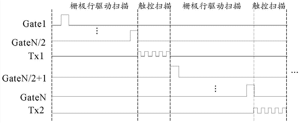
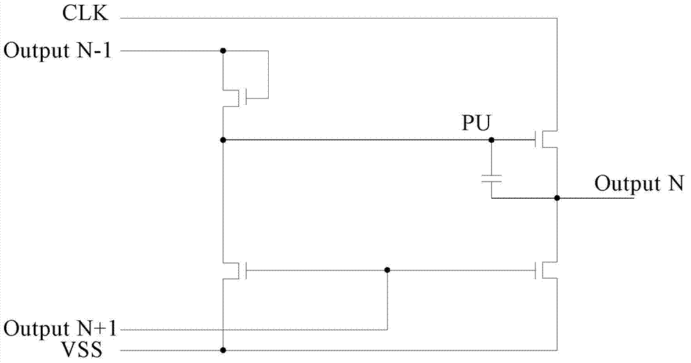
In the existing technology, such as image 3 As shown, the shift register unit takes the simplest 4T1C structure as an example, when the figure 1 During the H-Blank timing scan shown, since the N/2+1 row shift register unit is the first row of the second 1/2 display scan, but its pull-up control PU node outputs at row N/2 It has been charged to a high level, because there is a lon

Method used


Image

  • Gate drive circuit and method and display device
  • Gate drive circuit and method and display device
  • Gate drive circuit and method and display device

Examples


Embodiment Construction

[0031] The technical solutions in the embodiments of the present invention will be clearly and completely described below in conjunction with the accompanying drawings in the embodiments of the present invention. Obviously, the described embodiments are only a part of the embodiments of the present invention, rather than all the embodiments. Based on the embodiments of the present invention, all other embodiments obtained by a person of ordinary skill in the art fall within the protection scope of the present invention.

[0032] The transistors used in all the embodiments of the present invention can be thin film transistors or field effect transistors or other devices with the same characteristics. Since the source and drain of the transistors used here are symmetrical, there is no difference between the source and drain. of. In the embodiment of the present invention, in order to distinguish the two poles of the transistor other than the gate, one pole is called the first pole,...


PUM


Abstract

The invention provides a gate drive circuit and method and a display device and relates to the technical field of display. The method includes the steps that gate row drive scanning is performed on shifting register units located in a first area in the gate drive circuit; after gate row drive scanning of the shifting register units in the first area is finished, touch scanning is performed; after touch scanning is finished, the last-level shifting register unit located in the first area is scanned again so that the last-level shifting register unit located in the first area can be used for pre-charging a first-level shifting register unit located in a second area; gate row drive scanning is performed on shifting register units located in the second area in the gate drive circuit, and the last-level shifting register unit located in the first area is in cascade connection with the first-level shifting register located in the second area. The method can overcome the defect that the row pixel charging rate is insufficient and solve the problem of dark lines or poor bright lines.

Description

Technical field [0001] The present invention relates to the field of display technology, and in particular to a gate driving circuit, a driving method thereof, and a display device. Background technique [0002] With the increasing popularity of touch-sensitive display devices, people have higher and higher quality requirements for touch-sensitive display devices. In-cell touch technology is due to its thin thickness and touch sensitivity. It is widely used because of its high advantages. [0003] The in-cell touch technology means that the touch elements are integrated into the display panel, so that the panel itself has a touch function, and the touch effect and application can be achieved without additional bonding and assembly with the touch panel. Take a typical TFT-LCD (Thin Film Transistor-Liquid Crystal Display) as an example. Its characteristic is that the manufacturing technology of the touch sensing element is completed in the TFT-LCD standard manufacturing process, bec...

Claims


Application Information

Patent Timeline
IPC IPC(8): G09G3/20
CPCG06F3/0412G06F3/04184G06F3/044G09G3/3677G09G2310/0286G09G2320/0219G11C19/28G06F3/041G06F3/0416G09G2300/0426G09G2300/0809G09G2310/0251G09G2310/08
Inventor 张元波赵家阳韩承佑邹祥祥
Owner BOE TECH GRP CO LTD
Why Eureka
Try Eureka