Cavity cleaning method of plasma etching device

A technology of plasma and etching equipment, which is applied in the field of cavity cleaning of plasma etching equipment, can solve problems such as difficult cleaning, increase of agglomeration defects, and decrease of cleaning effect, so as to prolong residence time, optimize agglomeration defects, increase etch The effect of corrosion reaction

Active Publication Date: 2014-08-06
SHANGHAI HUALI MICROELECTRONICS CORP
View PDF8 Cites 16 Cited by
  • Summary
  • Abstract
  • Description
  • Claims
  • Application Information

AI Technical Summary

Problems solved by technology

Traditionally, when cleaning the reaction chamber, it is mostly carried out in a low vacuum pressure environment. However, the vacuum pumping device usually has a strong pumping capacity, and the plasma of the cleaning reaction gas may not fully react with the by-products. It is quickly drawn away from the reaction chamber by the vacuum pumping device, thereby redu

Method used


Image

  • Cavity cleaning method of plasma etching device
  • Cavity cleaning method of plasma etching device
  • Cavity cleaning method of plasma etching device

Examples


Example Embodiment

[0024] In order to make the content of the present invention clearer and easier to understand, the content of the present invention will be further described below in conjunction with the accompanying drawings. Of course, the present invention is not limited to this specific embodiment, and general replacements known to those skilled in the art are also covered within the protection scope of the present invention.

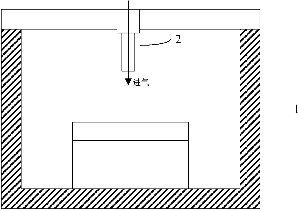
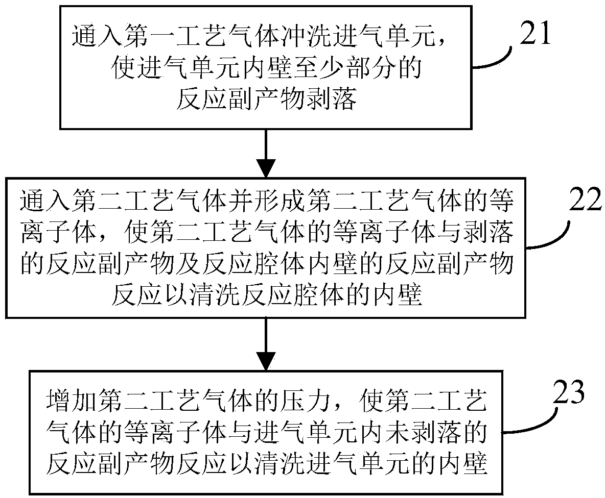
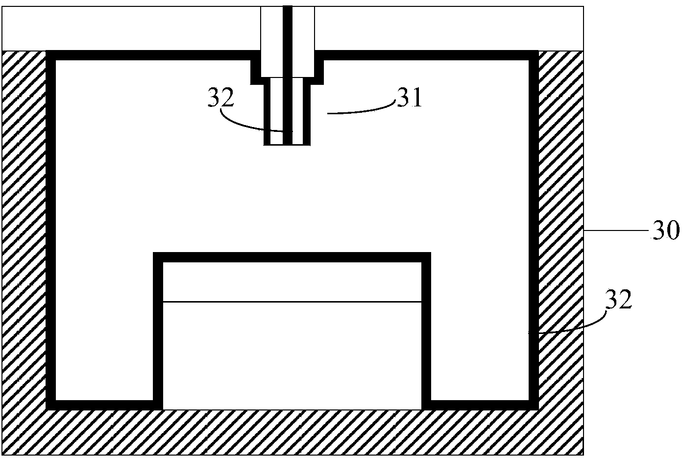
[0025] figure 2 shows a flow chart of the cavity cleaning method of the plasma etching device of the present invention, Figure 3a ~ 3f A cavity cleaning method of a plasma etching device provided in an embodiment of the present invention is shown. It should be understood that the plasma etching device in the figure is only exemplary, and it may include fewer or more constituent elements, or the arrangement of the constituent elements may be the same as Figure 3a ~ 3f shown differently.

[0026] like Figure 3a ~ 3f As shown, the plasma etching device include...


PUM


Abstract

The invention discloses a cavity cleaning method of a plasma etching device. The plasma etching device comprises a reaction cavity, a gas inlet unit and a gas exhaust unit. The cavity cleaning method includes the steps that first process gas is led into the plasma etching device to wash the gas inlet unit, and at least parts of reaction by-products on the inner wall of the gas inlet unit are peeled off; second process gas is led into the plasma etching device to form plasmas of the second process gas, and the second process gas reacts with the peeled-off reaction by-products and reaction by-products on the inner wall of the reaction cavity so as to clean the inner wall of the reaction cavity; the pressure of the second process gas is increased, so that the plasmas of the second process gas reacts with the unpeeled-off reaction by-products in the gas inlet unit so as to clean the inner wall of the gas inlet unit. The cavity cleaning method can effectively reduce the risk of wafer center agglomeration defects caused due to the fact that residues of the gas inlet unit deposit and fall.

Description

technical field [0001] The invention relates to the technical field of semiconductor processing, in particular to a cavity cleaning method of a plasma etching device. Background technique [0002] In recent years, with the development of semiconductor manufacturing technology, the requirements for the integration and performance of components are getting higher and higher. play a pivotal role. Generally speaking, in a plasma etching device, the plasma is generally formed by radio frequency excitation of the etching gas discharged from the inlet unit at the top of the reaction chamber, and the plasma bombards the wafer on the chuck, thereby realizing Etching of the wafer. [0003] figure 1 A schematic structural diagram of a plasma etching device is shown. The plasma processing device includes a reaction chamber 1 , and an air inlet unit 2 is connected to a reaction gas source (not shown in the figure) outside the reaction chamber, and is used to input the reaction gas pr...

Claims


Application Information

Patent Timeline
IPC IPC(8): B08B9/08
CPCB08B9/08B08B9/093
Inventor 许进段智公任昱吕煜坤
Owner SHANGHAI HUALI MICROELECTRONICS CORP
Why Eureka
Try Eureka