Manufacturing apparatus of electric part, manufacturing method of electric part and manufacturing method of LED illumination

A technology for electronic components and manufacturing methods, applied in the direction of assembling printed circuits with electrical components, printed circuit manufacturing, electrical components, etc., can solve the problems of deterioration of fluorescent agents, deformation of substrates, adverse effects of electronic components, etc., and achieve the effect of suppressing damage

Inactive Publication Date: 2014-08-20
NISSHINBO MECHATRONICS
View PDF2 Cites 12 Cited by
  • Summary
  • Abstract
  • Description
  • Claims
  • Application Information

AI Technical Summary

Problems solved by technology

Therefore, there will be the following problems: the substrate will be deformed to affect the quality, high temperature will cause adverse effects on electronic components, and when the substrate is long, a large and long reflow oven is required
Regarding adverse effects on electronic components, when the electronic component is an LED, if it is exposed to the high heat of a reflow oven for a long time, the fluorescent agent in the LED part will deteriorate and sufficient brightness will not be obtained.

Method used


Image

  • Manufacturing apparatus of electric part, manufacturing method of electric part and manufacturing method of LED illumination
  • Manufacturing apparatus of electric part, manufacturing method of electric part and manufacturing method of LED illumination
  • Manufacturing apparatus of electric part, manufacturing method of electric part and manufacturing method of LED illumination

Examples


Embodiment 1

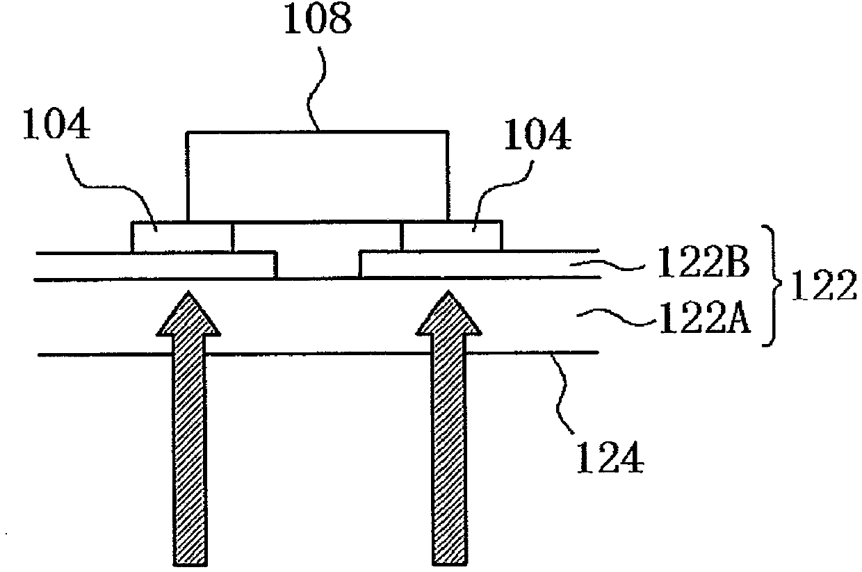
[0098] In Example 1, a substrate made of PET was used, and in Example 2, a substrate made of PEN was used. First, on each substrate, a copper foil is etched by a known method to form a wiring pattern, thereby producing a printed circuit board. Both the substrates used in Example 1 and Example 2 had a thickness of 50 μm and were flexible.

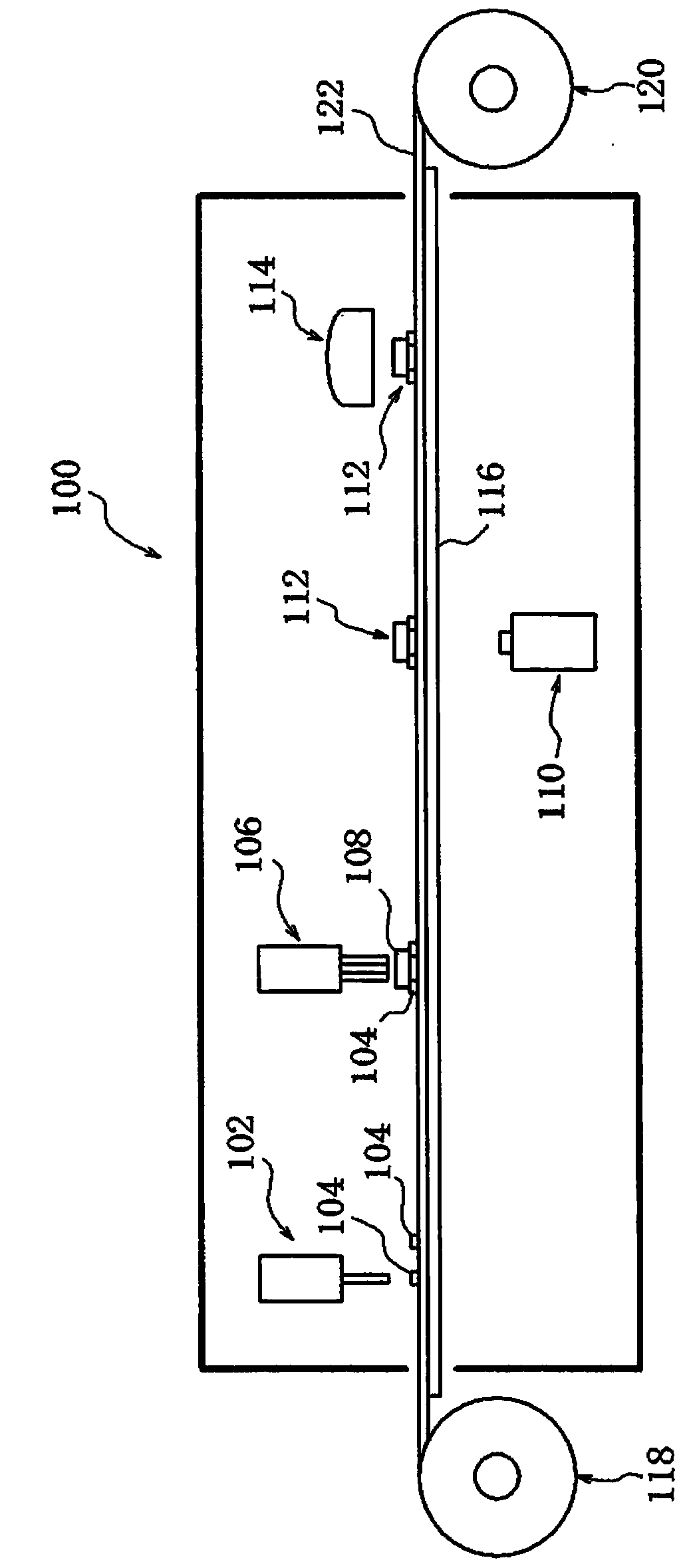
[0099] Second, use figure 1 In the illustrated reel-to-reel electronic component manufacturing apparatus, LEDs are mounted while winding a substrate from one reel to the other reel. Using a non-contact jet applicator (JetMaster: manufactured by Musashi High-Tech Co., Ltd.), paste solder was supplied onto the wiring pattern of the printed circuit board. Then, an LED element was mounted on the cream solder using a mounter (desk mounter: manufactured by Okuhara Electric Co., Ltd.). Secondly, use a semiconductor laser device with a luminous center wavelength of 920nm (LD irradiation device 15W type: manufactured by Japan Hamamatsu Photonics ...


PUM

PropertyMeasurementUnit
emission peakaaaaaaaaaa

Abstract

Provided are an apparatus for manufacturing an electronic part and a method of manufacturing the electronic part, wherein an electronic element can be soldered to a printed circuit board in a shorter time than conventional methods, and wherein damage to the electronic element, spattering of solder, and damage to the circuit board can be inhibited. An apparatus (100) for manufacturing an electronic part (112) according to the present invention, which mounts an electronic element (108) on a printed circuit board (122) comprising a substrate (122A) and a wiring pattern (122B) disposed thereon, comprises: a supplying apparatus (102) that supplies solder (104) onto the wiring pattern (122B) of the printed circuit board (122); a placing apparatus (106) that places the electronic element (108) on the solder (104); a laser (112) that radiates light having the center wavelength of the light-emission thereof within a range of 700 nm - 1100 nm, towards the solder (104) upon which the electronic element (108) is mounted, from the back face (124) side of the printed circuit board. The apparatus (100) for manufacturing an electronic part (112) is characterized in that the light transmits through the substrate (122A) to reach the wiring pattern (122B), heats the wiring pattern (122B) and melts the solder (104), so that the electronic element (108) is soldered to the printed circuit board (122).

Description

technical field [0001] The present invention relates to a manufacturing apparatus for manufacturing electronic parts by mounting electronic components on a printed circuit board, a method for manufacturing electronic parts, and a method for manufacturing an LED lighting device including processes of the manufacturing method. Background technique [0002] When manufacturing electronic components by mounting electronic components on a printed circuit board having a substrate and a wiring pattern provided on the substrate, a reflow method is a mainstream method for soldering electronic components to the printed circuit board. In the reflow soldering method, the electronic components are placed on the wiring pattern on the surface of the printed circuit board through the intermediary solder, and then the printed circuit board is transported to the reflow soldering furnace, and hot air of a specified temperature is blown to the printed circuit board in the reflow soldering furnace...

Claims


Application Information

Patent Timeline
Patent Type & Authority Applications(China)
IPC IPC(8): H05K3/34
CPCH05K3/3494H05K2201/10106H05K2203/107H05K2201/0145H05K2203/1581H01L2224/81224
Inventor 池田恒平冨田秀司塚本奈巳
Owner NISSHINBO MECHATRONICS
Why Eureka
Try Eureka