Grid drive circuit of flat-panel display and low-power-consumption output module thereof
A gate drive circuit, flat panel display technology, applied in static indicators, instruments, etc., can solve the problems of difficulty in ensuring signal integrity, complex driving principles, and multiple glass areas, and achieve simple structure, simple peripheral driving, and glass area. small effect
- Summary
- Abstract
- Description
- Claims
- Application Information
AI Technical Summary
Problems solved by technology
Method used
Image

Examples
Embodiment 1
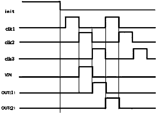
[0046] figure 1 It is a schematic diagram of a multi-level gate driving circuit in this embodiment, and the gate driving circuit includes a plurality of cascaded driving units. Such as figure 2 As shown, each driving unit includes transistors T101-T115 and capacitors C101-C102;
[0047] The gate of the transistor T103 and the gate of the transistor T104 are respectively connected to the clock signal line CLK1; the drain of the transistor T3 is connected to the power line VDD; the source of the transistor T3 is connected to the drain of the transistor T4; the source of the transistor T104 is respectively connected to the The drain of the transistor T105, the drain of the transistor T111, the first end of the capacitor C102, the gate of the transistor T108, and the gate of the transistor T110 are connected; the gate of the transistor T105 and the gate of the transistor T106 are respectively connected to the signal input terminal VIN The source of the transistor T105 is connec...
Embodiment 2
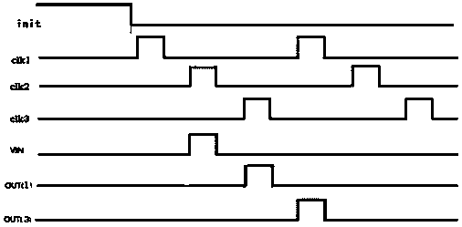
[0063] The gate drive circuit of this embodiment includes a plurality of cascaded drive units, such as Figure 5 As shown, each driving unit includes transistors T201-T216 and capacitors C201-C202;
[0064] The gate of the transistor T203 and the gate of the transistor T204 are respectively connected to the first clock signal line CLK1; the drain of the transistor T203 is connected to the first power line VDD; the source of the transistor T203 is connected to the drain of the transistor T204; the drain of the transistor T204 The source is respectively connected to the drain of the transistor T205, the drain of the transistor T211, the first end of the capacitor C202, the gate of the transistor T208, and the gate of the transistor T210; the gate of the transistor T205 and the gate of the transistor T206 are respectively connected to the input The terminal VIN is connected; the source of the transistor T205 is connected to the drain of the transistor T206; the source of the tran...
Embodiment 3
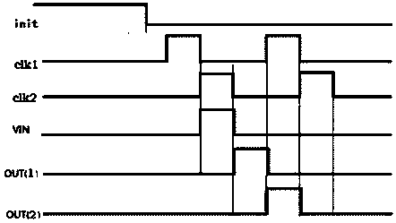
[0075] The gate drive circuit of this embodiment includes a plurality of cascaded drive units, such as Figure 7 As shown, each driving unit includes each driving unit includes transistors T301-T313 and a first capacitor;
[0076] The drain of the transistor T303 is connected to the first power line VDD; the gate of the transistor T303, the gate of the transistor T301, the gate of the transistor T302, and the source of the transistor T304 are respectively connected to the first clock signal line CLK1; the source of the transistor T303 , the drain of the transistor T304, the drain of the transistor T310, and the gate of the transistor T306 are respectively connected to the gate of the transistor T308; the gate of the transistor T304, the source of the transistor T302, the drain of the transistor T311, and the gate of the transistor T305 respectively connected to the first end of the first capacitor;
[0077] The drain of the transistor T301 is connected to the input terminal V...
PUM
 Abstract
Description
Claims
Application Information