Reworking method for LED epitaxial wafer with distributed Bragg reflector (DBR)

A technology of Bragg reflectors and light-emitting diodes, which is applied to electrical components, circuits, semiconductor devices, etc., can solve problems such as easy breakage, manufacturer cost loss, and large warpage, so as to avoid breakage, cost loss, The effect of saving manufacturing cost

Active Publication Date: 2014-09-03
HC SEMITEK SUZHOU
View PDF6 Cites 7 Cited by
  • Summary
  • Abstract
  • Description
  • Claims
  • Application Information

AI Technical Summary

Problems solved by technology

[0004] In the process of realizing the present invention, the inventor has found that the prior art has at least the following problems: when removing the dirty DBR film layer on the 4-inch epitaxial wafer by grinding, due to the warpage of the 4-inch epitaxial wafer than the two-inch epitaxial wafer Therefore, it is very easy to break during the grinding process, resulting in the direct scrapping of the epitaxial wafer, which brings cost loss to the manufacturer

Method used


Image

  • Reworking method for LED epitaxial wafer with distributed Bragg reflector (DBR)
  • Reworking method for LED epitaxial wafer with distributed Bragg reflector (DBR)
  • Reworking method for LED epitaxial wafer with distributed Bragg reflector (DBR)

Examples


Embodiment 1

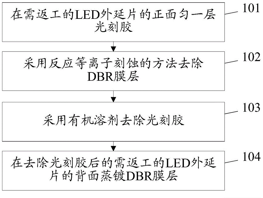
[0038] An embodiment of the present invention provides a method for reworking a light-emitting diode epitaxial wafer equipped with a distributed Bragg reflector, see figure 2 , the method includes:

[0039] Step 101: Spread a layer of photoresist on the front surface of the LED epitaxial wafer to be reworked.

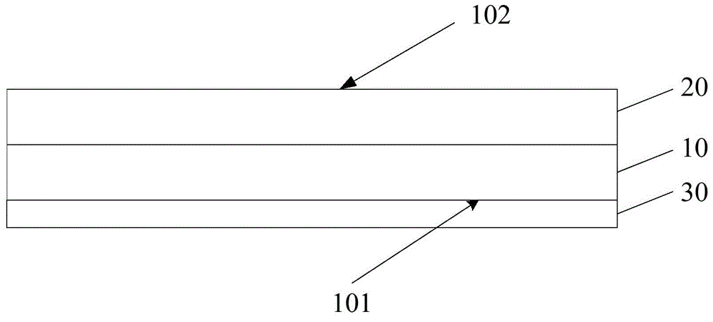
[0040] Wherein, the back side of the LED epitaxial wafer to be reworked is provided with a DBR film layer, and the DBR film layer is dirty.

[0041] Step 102: Removing the DBR film layer by reactive plasma etching (Reactive Ion Etching, RIE for short).

[0042] Among them, the etching power is 400-700W, the etching pressure is 20-30mtorr, the etching temperature is 0-10°C, the etching thickness is greater than the thickness of the DBR film layer, and the etching gas is 50-80 sccm of CHF 3 and O 2 .

[0043] Step 103: removing the photoresist by using an organic solvent.

[0044] Step 104: Evaporating a DBR film layer on the backside of the LED epitaxial wafer to b...

Embodiment 2

[0048] An embodiment of the present invention provides a method for reworking a light-emitting diode epitaxial wafer equipped with a distributed Bragg reflector, see image 3 , the method flow includes:

[0049] Step 201: Spread a layer of photoresist on the front surface of the LED epitaxial wafer to be reworked.

[0050] Wherein, the back side of the LED epitaxial wafer to be reworked is provided with a DBR film layer, and the DBR film layer is dirty.

[0051] As an optional manner of this embodiment, the thickness of the photoresist may be 5um˜10um.

[0052] First, the LED epitaxial wafer to be reworked is fixed on the supporting member, and the supporting member drives the LED epitaxial wafer to rotate, and the rotational speed may be 800 rpm. Then adopt the method of manual glue spreading to spread a layer of photoresist on the front side of the rotating LED epitaxial wafer to be reworked.

[0053] Step 202: Using RIE to remove the DBR film layer.

[0054] Among them,...


PUM


Abstract

The invention discloses a reworking method for an LED epitaxial wafer with a DBR, belonging to the LED field. The method comprises that the front side of the LED epitaxial wafer which needs reworking is uniformly provided with a layer of photoresist, and the back side of the LED epitaxial layer is provided with a DBR film layer; the DBR film layer is removed in an RIE (Reactive Ion Etching) manner, the etching power ranges from 400 to 700 W, the etching pressure ranges from 20 to 30 mtorr, the etching temperature ranges from 0 to 10 DEG C, the etching thickness is greater than the thickness of the DBR film layer, and etching gas includes CHF3 and O2 of 50-80 sccm; the photoresist is removed via an organic solvent; and the back side of the LED epitaxial wafer from which the photoresist is removed is provided with a DBR film layer in a vapor plating manner. According to the reworking method, the DBR film layer at the back side of the LED epitaxial wafer which needs reworking is removed in the RIE manner, and the RIE manner includes gas etching, so that the LED epitaxial layer is avoided from fragmentation and further loss caused by grinding.

Description

technical field [0001] The invention relates to the field of light emitting diodes (Light Emitting Diode, LED for short), in particular to a method for reworking light emitting diode epitaxial wafers equipped with distributed Bragg reflectors. Background technique [0002] With the maturity of LED epitaxy and chip technology, it has become a method for LED chip manufacturers to improve the light extraction efficiency of high-power chips by evaporating distributed Bragg Reflection (DBR) on the back of LED epitaxial wafers. The process that the businessman pays attention to. [0003] In the actual mass production process, the LED epitaxial wafers need to be waxed and cleaned after the thinning process. Due to the fact that organic particles are often not cleaned during the cleaning process, after the cleaned LED epitaxial wafer is evaporated with DBR, the evaporated DBR film layer is dirty in a large area. For products with dirty DBR film layer, rework is required. The trad...

Claims


Application Information

Patent Timeline
Patent Type & Authority Applications(China)
IPC IPC(8): H01L33/46H01L33/00
CPCH01L21/31138H01L33/46
Inventor 周武胡根水
Owner HC SEMITEK SUZHOU
Why Eureka
Try Eureka