

Touch Sensor-Embedded Display Panel, Display Device Provided Therewith, And Method For Driving Touch Sensor-Embedded Display Panel
一种触摸传感器、显示面板的技术,应用在仪器、静态指示器、数据处理的输入/输出过程等方向,能够解决重量和厚度触摸面板电力增加等问题,达到抑制显示动作性能和触摸检测动作性能的降低、抑制开口率的降低、降低负荷的效果
- Summary
- Abstract
- Description
- Claims
- Application Information
AI Technical Summary
Problems solved by technology
Method used
Image


Examples
no. 1 approach
[0099]
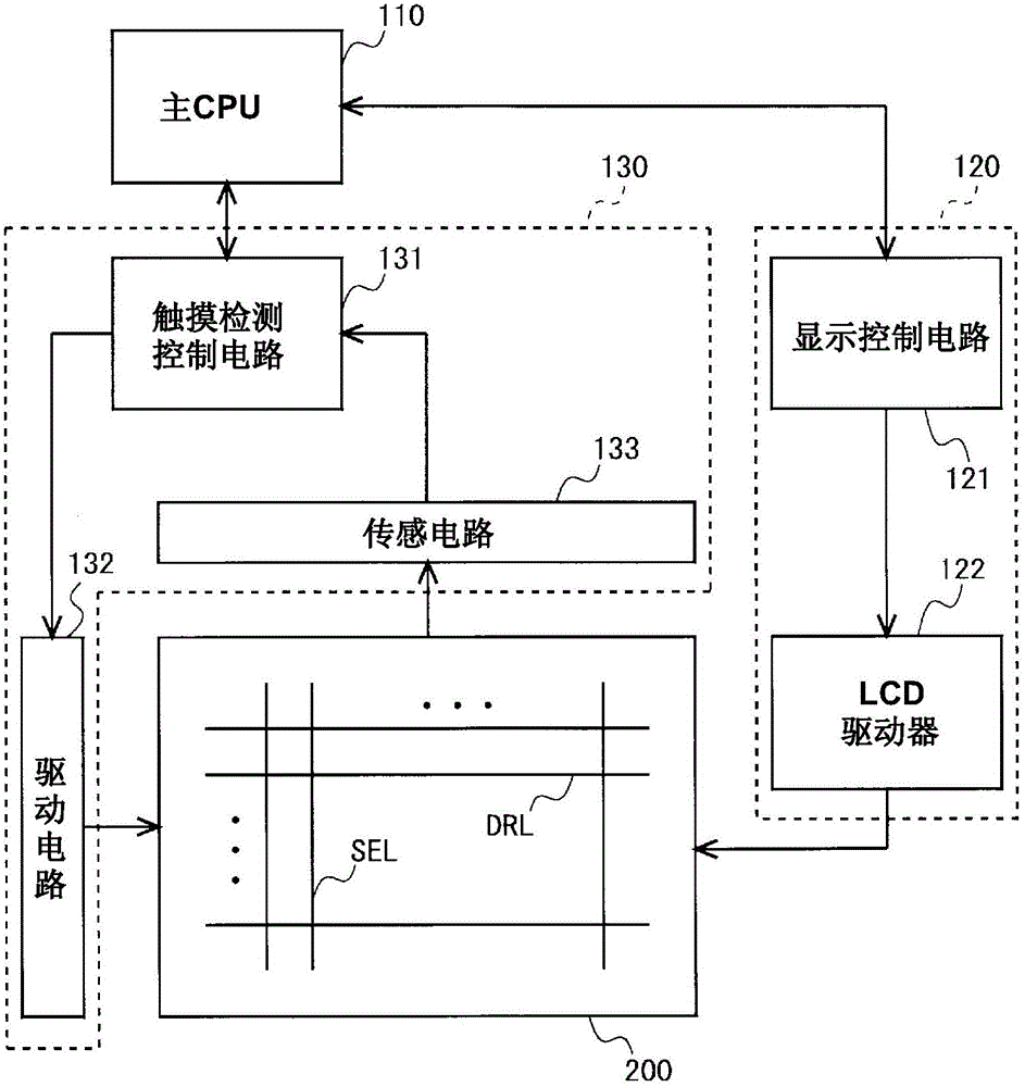
[0100] figure 1 It is a block diagram showing the overall configuration of the liquid crystal display device according to the first embodiment of the present invention. The present liquid crystal display device not only has the image display function originally provided by the liquid crystal display device, but also has a touch sensor function. This liquid crystal display device, such as figure 1 As shown, main CPU 110 , display control unit 120 , touch detection control unit 130 , and touch sensor built-in liquid crystal display panel 200 (hereinafter simply referred to as “display panel 200 ”) are provided. The display control unit 120 includes a display control circuit 121 and an LCD driver 122 . The touch detection control unit 130 includes a touch detection control circuit 131 , a driving circuit 132 and a sensing circuit 133 . In addition, although not shown, a backlight is provided on the rear surface of the display panel 200 .
[0101] In the display p...
no. 2 approach
[0147]
[0148] Figure 13 It is a diagram showing a part of the common electrode pattern on the CF substrate 28 in the second embodiment of the present invention. In addition, in this embodiment, except for the common electrode pattern, the structure and the like are basically the same as those of the above-mentioned first embodiment, and therefore description of such common parts will be omitted. Such as Figure 13 As shown, the sensing line SEL in this embodiment is formed by electrically connecting a plurality of substantially diamond-shaped regions 41 arranged in the Y direction to each other. In the present embodiment, the substantially diamond-shaped region 41 forming the sensing line SEL is referred to as a "sensing segment". In addition, the drive line DRL is formed by electrically connecting a plurality of substantially rhombic 42 arranged in the X direction to each other. In the present embodiment, the diamond-shaped region 42 forming the drive line DRL is refe...
no. 3 approach
[0153]
[0154] Before describing the third embodiment of the present invention, prior art related to the third embodiment will be described. Figure 15 It is an equivalent circuit diagram showing a pixel structure in a conventional liquid crystal display device employing a multi-pixel structure. also, Figure 15 The pixel structure shown is disclosed in, for example, Non-Patent Document 1. Here, the "multi-pixel structure" refers to a structure in which one pixel is divided into a plurality of (typically two) sub-pixels in order to eliminate the viewing angle dependence of the gamma characteristic of a liquid crystal display panel such as a VA system. In addition, the "one pixel" mentioned here is actually equivalent to the "one sub-pixel" mentioned in the above-mentioned first embodiment, and the "sub-pixel" mentioned here is a reference to the above-mentioned first embodiment. It is obtained by dividing the "sub-pixels". However, here, for the sake of convenience, it i...
PUM
 Abstract
Description
Claims
Application Information