Photovoltaic element and manufacturing method thereof

A photovoltaic element and protective layer technology, applied in the field of photovoltaic elements and its manufacturing, can solve the problem of increasing the reflectivity of the anti-reflection layer and achieve the effect of suppressing the PID effect

Inactive Publication Date: 2016-03-16
SINO AMERICAN SILICON PROD
View PDF2 Cites 0 Cited by
  • Summary
  • Abstract
  • Description
  • Claims
  • Application Information

AI Technical Summary

Problems solved by technology

However, this method will slightly sacrifice the efficacy of the anti-reflection layer itself, that is, the reflectivity of the anti-reflection layer will increase.
Moreover, this approach is not necessarily applicable to other types of photovoltaic components

Method used


Image

  • Photovoltaic element and manufacturing method thereof
  • Photovoltaic element and manufacturing method thereof
  • Photovoltaic element and manufacturing method thereof

Examples


Embodiment Construction

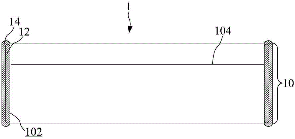
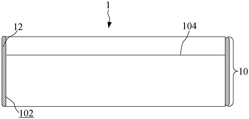
[0019] see figure 1 , figure 1 A photovoltaic element 1 according to a preferred embodiment of the present invention is schematically shown in a cross-sectional view.

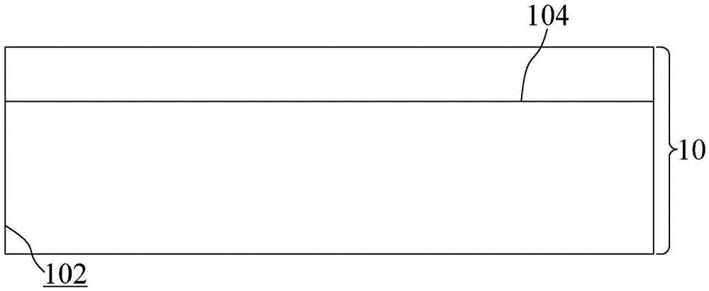
[0020] Such as figure 1 As shown, the photovoltaic element 1 of the present invention includes a semiconductor structure combination 10 and a first protective layer 12 . The semiconductor structure assembly 10 has multiple side surfaces 102 and includes p-n junctions, n-p junctions, p-i-n junctions, n-i-p junctions, double junctions, multiple junctions, or other types of junctions. That is to say, the photovoltaic element 1 of the present invention can be a monocrystalline silicon photovoltaic element, a quasi-monocrystalline silicon photovoltaic element, a polycrystalline silicon photovoltaic element, a gallium arsenide-based photovoltaic element, an amorphous silicon thin film photovoltaic element, a microcrystalline silicon (μ-Si ) thin film photovoltaic elements, cadmium sulfide (CdS) thin film photovolt...


PUM


Abstract

The present invention provides a photovoltaic element and a manufacturing method thereof. The photovoltaic element comprises a semiconductor structure composition and a protection layer. The semiconductor structure composition comprises a plurality of side surfaces, a p-n junction, an n-p junction, a p-i-n junction, an n-i-p junction, a double junction and a multiple junction. In particular, the protection layer is formed to cover the plurality of side surfaces of the semiconductor structure composition. Therefore, the protection layer is allowed to prevent the photovoltaic element from generating a potential induced attenuation effect.

Description

technical field [0001] The present invention relates to a photovoltaic element and a manufacturing method thereof, and in particular, to a photovoltaic element capable of effectively suppressing potential-induced degradation (PID) effect and a manufacturing method thereof. Background technique [0002] Recently, the reliability of photovoltaic elements and their packaging modules caused by the PID effect has been paid more and more attention. Photovoltaic component manufacturers are all committed to developing photovoltaic components and their packaging modules that can suppress the PID effect. The PID effect was first discovered in 2005 by Sunpower in n-type silicon-based photovoltaic components. The packaging module has been exposed to high temperature, humidity and high voltage for a long time, so that there is leakage current between the glass and the packaging material, and a large amount of charge accumulates on the surface of the photovoltaic element, which deteriora...

Claims


Application Information

Patent Timeline
Patent Type & Authority Patents(China)
IPC IPC(8): H01L31/0216H01L31/04H01L31/18
CPCH01L31/02167H01L31/02168H01L31/022425H01L31/1804Y02E10/547Y02P70/50
Inventor 布迪·贾约诺杨明瑞丁传文邱玉婷谭任廷吴文生沈国伟胡芳维
Owner SINO AMERICAN SILICON PROD
Why Eureka
Try Eureka