A kind of preparation method of crystalline silicon solar cell

A technology of solar cells and crystalline silicon, applied in the field of solar energy, can solve the problems of increasing the cost of solar modules, limited selection of inverters, adverse effects on system efficiency, etc. Simple and easy method

Active Publication Date: 2016-04-13
CSI CELLS CO LTD
View PDF5 Cites 0 Cited by
  • Summary
  • Abstract
  • Description
  • Claims
  • Application Information

AI Technical Summary

Problems solved by technology

[0004] In view of the above problems, the existing anti-potential-induced attenuation methods mainly include the following: (1) avoiding the formation of a negative potential difference (front n-type emitter) and a positive potential difference between the solar module frame and the solar cells contained in the solar module. Poor (front p-type emitter), such as grounding, but the related grounding measures may be extremely complicated, in addition to restricting the choice of inverters, which will have a negative impact on system efficiency; (2) using A glass plate made of borosilicate glass, because borosilicate glass will promote charge accumulation is relatively less ion components, however, this will increase the cost of solar modules, which is an unacceptable solution from an economic point of view; (3) try to use More suitable materials than EVA to make plastic films, such as silicone (such as Tectosil from blacker company), PVB polyvinyl butyral or thermoplastics (such as Surlyn from Dupont company), because the acetic acid contained in EVA and the High water and moisture permeability can be detrimental; however, EVA films are well suited for use in solar modules for a variety of reasons that cannot be achieved with films of other materials mentioned above

Method used


Image

  • A kind of preparation method of crystalline silicon solar cell
  • A kind of preparation method of crystalline silicon solar cell

Examples


Embodiment 1

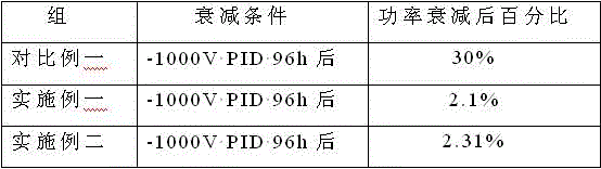
[0029] A method for preparing a crystalline silicon solar cell, taking the preparation of an existing conventional cell as an example, comprises the following steps:

[0030] (1) Texturing, diffusion, and edge etching of the silicon wafer;

[0031] (2) Form a silicon dioxide dielectric film on the light-receiving surface of the silicon wafer by PECVD, and the silicon oxide thickness is 2.2nm;

[0032] (3) Plating anti-reflection film, printing electrodes by screen printing, and sintering to form ohmic contact;

[0033] (4) Using conventional packaging materials, the battery strings are interconnected, packaged, and laminated to make components.

Embodiment 2

[0035] A method for preparing a crystalline silicon solar cell, taking the preparation of an existing conventional cell as an example, comprises the following steps:

[0036] (1) Texturing, diffusion, and edge etching of the silicon wafer;

[0037] (2) Form a silicon dioxide dielectric film on both sides of the silicon wafer by PECVD, and the silicon dioxide thickness is 2.2nm;

[0038] (3) Plating anti-reflection film, printing electrodes by screen printing, and sintering to form ohmic contact;

[0039] (4) Using battery sheets with the same efficiency level as in Example 1 and conventional packaging materials, the battery strings are interconnected, packaged, and laminated to make components.

Embodiment 3

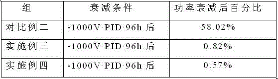
[0050] A method for preparing a crystalline silicon solar cell, taking the preparation of a MWT cell as an example, comprises the following steps:

[0051] (1) Texturing, diffusion, and edge etching of the silicon wafer;

[0052] (2) Form a silicon dioxide dielectric film on the light-receiving surface of the silicon wafer by PECVD, and the silicon oxide thickness is 2.5nm;

[0053] (3) Plating anti-reflection film, drilling, printing electrodes by screen printing, and sintering to form ohmic contact;

[0054] (4) Using conventional packaging materials, the battery strings are interconnected, packaged, and laminated to make components.


PUM

PropertyMeasurementUnit
thicknessaaaaaaaaaa
thicknessaaaaaaaaaa
thicknessaaaaaaaaaa

Abstract

Disclosed is a method for preparing a crystalline silicon solar cell. The method comprises the following steps: (1) cleaning the surface of a silicon slice, and performing texturing, diffusion, junction making and edge etching on the surface of the silicon slice; (2) forming a layer of silicon dioxide dielectric film on a light-receiving surface or a double surfaces of the silicon slice, the thickness of the layer of silicon dioxide dielectric film is 1.0 to 10 nm; and (3) performing antireflective film coating, silk-screen printing and sintering to obtain the crystalline silicon solar cell. In this way, a method for preparing a crystalline silicon solar cell resisting potential induced degradation is developed. The formed silicon dioxide dielectric film well blocks ion migration, prevents the ion migration from damaging a PN junction and effectively restrains a PID effect and can meet requirements on a PID Free cell plate.

Description

technical field [0001] The invention relates to a preparation method of a crystalline silicon solar cell, which belongs to the technical field of solar energy. Background technique [0002] A solar cell, also known as a photovoltaic cell, is a semiconductor device that converts the sun's light energy directly into electrical energy. Because it is a green product, does not cause environmental pollution, and is a renewable resource, solar cells are a new energy source with broad development prospects in today's energy shortage situation. [0003] It is well known that when a solar module in a solar module string of one or more solar modules operates, a potential is formed between the solar cell and the frame. If the solar cells in a solar module are connected in series, the potential between the solar cells and the frame rises along this series line. The limit value proposed by the industry for this potential is usually about 1000 volts, ie a potential of around 1000 volts i...

Claims


Application Information

Patent Timeline
Patent Type & Authority Patents(China)
IPC IPC(8): H01L31/18
CPCH01L31/02363H01L31/02168H01L31/068Y02E10/547
Inventor 王栩生张春华周剑辛国军章灵军
Owner CSI CELLS CO LTD
Why Eureka
Try Eureka