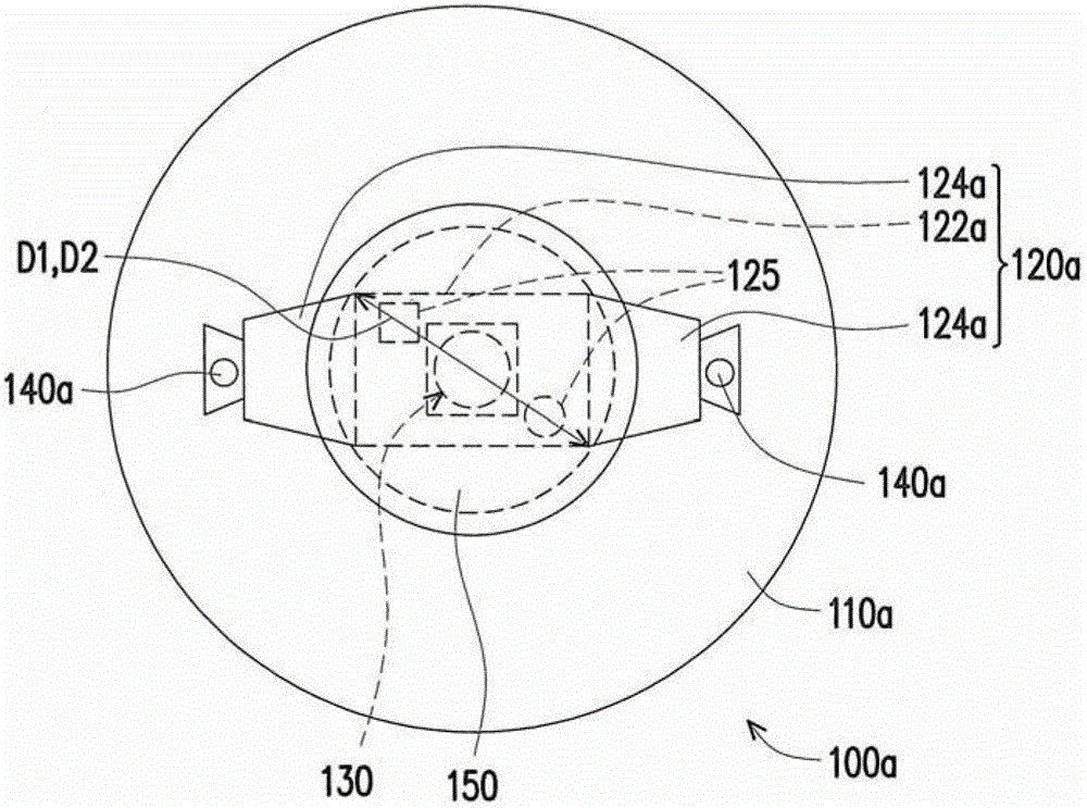
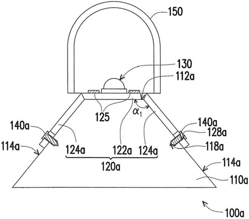
[0039] figure 1 It is a schematic top view of a light emitting device according to an embodiment of the present invention. figure 2 for figure 1 A schematic cross-sectional view of the light emitting device shown. Please also refer to figure 1 versus figure 2 In this embodiment, the light emitting device 100a includes a carrier 110a, a substrate 120a, and at least one electrode pair 125 ( figure 1 versus figure 2 A pair is schematically shown in), at least one light-emitting diode 130 ( figure 1 versus figure 2 Schematically shows one) and at least one positioning member 140a ( figure 1 versus figure 2 Two are shown schematically in ).
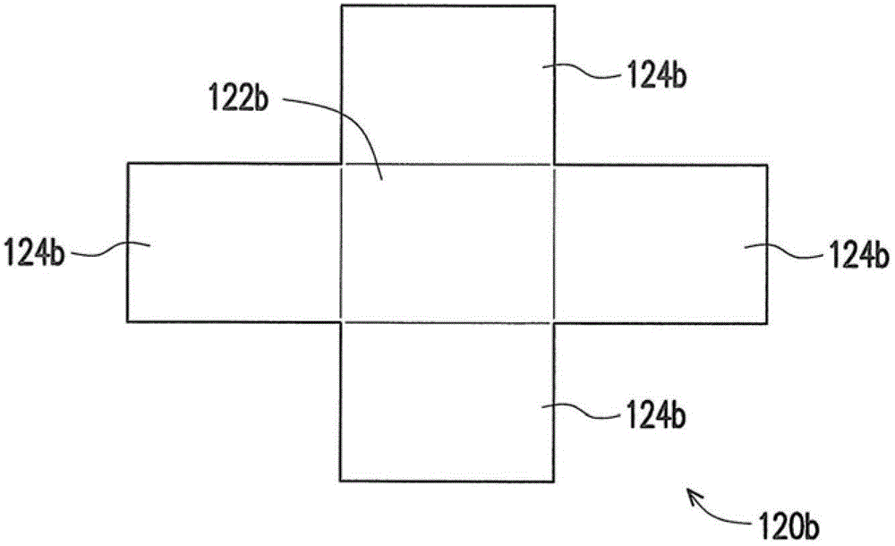
[0040] In detail, the substrate 120a is disposed on the carrier 110a, and has a body portion 122a and at least one bending portion 124a ( figure 1 Two are schematically shown in ), in which the bent portion 124a is connected to the body portion 122a. In particular, the bent portion 124a and the body portion 122a are not coplanar. The electrode pair 125 is arranged on the main body 122a of the substrate 120a. The light emitting diode 130 is disposed on the main body 122a of the substrate 120a and is electrically connected to the electrode pair 125. The positioning member 140a is disposed on the bent portion 124a of the substrate 120a, and is used to fix the substrate 120a on the carrier 110a.
[0041] More specifically, the carrier 110a of this embodiment is, for example, a heat sink, which can be made of a material with good thermal conductivity, such as copper, aluminum, or ceramic. The substrate 120a is, for example, a flexible substrate, wherein the body portion 122a of the substrate 120a is disposed on a top surface 112a of the carrier 110a, and the bent portion 124a of the substrate 120a is disposed on the side surface of the carrier 110a connected to the top surface 112a On 114a. Such as figure 1 As shown, the shape of the substrate 120a is, for example, a belt shape. Of course, in other embodiments, please refer to image 3 The shape of the substrate 120b can also be a cross shape, that is, the substrate 120b has four bending portions 124b connected to the body portion 122b. This still belongs to the applicable technical solution of the present invention and does not deviate from the protection scope of the present invention.
[0042] Such as figure 2 As shown, there is an included angle α between the body portion 122a and the bending portion 124a of the substrate 120a of this embodiment. 1 , And the included angle α 1 Between 90 degrees and 150 degrees. In other embodiments, please refer to Figure 4 , The main body portion 122c of the substrate 120c and the bending portion 124c have an included angle α 2 , Where the included angle α 2 90 degrees, this design also has the effect of letting out the light angle greater; or, in other unshown embodiments, the angle between the body portion of the substrate and the bending portion can also be less than 90 degrees , But considering the circuit design and heat dissipation effect, the angle should not be less than 30 degrees. More specifically, preferably, the included angle between the body portion 122a of the substrate 120a and the bending portion 124a is between 30 degrees and 150 degrees. In addition, because the positioning member 140a is disposed on the bent portion 124a of the substrate 120a, the body portion 122a can reduce the area reserved for the locking screw of the existing light-emitting device, so that the overall area and volume of the light-emitting device 100a are also changed accordingly. Small, so it can have a more flexible configuration space. More preferably, the area of the main body 122a is 1.05 to 1.3 times the area of the light emitting diode 130. The above-mentioned technology still belongs to the applicable technical solutions of the present invention, and does not deviate from the scope of protection of the present invention.
[0043] Furthermore, the carrier 110a of this embodiment includes at least one first positioning hole 118a ( figure 2 Two are shown schematically in the middle), and the substrate 120a includes at least one second positioning hole 128a ( figure 2 Two are shown schematically in). The second positioning hole 128a is located on the bending portion 124a. The positioning member 140a passes through the second positioning hole 128a and the first positioning hole 118a to fix the substrate 120a on the carrier 110a. Here, the positioning member 140a is, for example, a screw, and both the first positioning hole 118a and the second positioning hole 128a are, for example, screw holes.
[0044] In addition, the light emitting device 100a of this embodiment may further include a mask 150, wherein the mask 150 is disposed on the main body 122a of the substrate 120a and covers the light emitting diode 130 and the electrode pair 125. The mask 150 is, for example, a fluorescence conversion mask, and its purpose is to convert the wavelength of part of the light emitted by the light emitting diode 130. Here, such as figure 1 As shown, the orthographic projection area of the mask 150 on the main body 122a of the substrate 120a is larger than the surface area of the main body 122a of the substrate 120a. Of course, in other embodiments not shown, the orthographic projection area of the mask 150 on the main body 122a of the substrate 120a may also be equal to the surface area of the main body 122a of the substrate 120a. In addition, the maximum distance D1 between two points in the opening of the mask 150 is equal to the maximum distance between two points on the edge of the body portion 122a of the substrate 120a. Here, the maximum distance between two points on the edge of the main body portion 122a of the substrate 120a is the diagonal length D2 of the main body portion 122a.
[0045] Since the body portion 122a and the bending portion 124a of the substrate 120a of this embodiment are not coplanar, when the positioning member 140a locks the carrier 110a and the substrate 120a, compared with the existing electrode pair and the locking screw are located on the same plane. In other words, the distance between the electrode pair 125 and the positioning member 140a of this embodiment can be effectively increased. That is, the positioning member 140a and the electrode pair 125 electrically connected to the light emitting diode 130 are effectively isolated. In this way, the arc effect caused by mutual induction between the electrode pair 125 and the positioning member 140a can be prevented, and the short circuit can be avoided, thereby increasing the number of times the light emitting device 100a of the present embodiment passes the high voltage test and is more in compliance with safety regulations. Requirements. In addition, the heat emitted by the light-emitting diode 130 of this embodiment can also be transferred to the bending portion 124a through the design of the substrate 120a, and then conduct heat through the carrier 110a to avoid heat accumulation on the body portion 122a, which can effectively improve the light-emitting device 100a heat dissipation effect.
[0046] It is worth mentioning that the present invention does not limit the shape of the carrier 110a, although the carrier 110a mentioned here is embodied as a trapezoidal heat sink. However, in other unshown embodiments, the carrier 110a can also be a heat dissipation fin, a heat dissipation plate, a heat conduction column or a heat pipe, which still belongs to the technical solution that can be used in the present invention and does not deviate from the present invention. The scope of the desired protection. Furthermore, the present invention does not limit the structure of the first positioning hole 118a, the second positioning hole 128a, and the positioning member 140a, although the first positioning hole 118a, the second positioning hole 128a, and the positioning member 140a mentioned here are specifically They are screw holes, screw holes and screws. However, in other unshown embodiments, the first positioning hole 118a and the second positioning hole 128a may also be a combination of two of the screw holes, through holes, and blind holes, and the positioning member 140a may also be Bolts or rivets. Alternatively, since the body portion 122a and the bending portion 124a of the substrate 120a are not coplanar, a more elastic fixing method of the positioning member 140a is provided without being restricted by the safety distance from the electrode pair 125 and the surface area of the substrate 120a. In more detail, in addition to fixing the substrate 120a on the carrier 110a by screw locking, the positioning member 140a can also be fixed by a buckle or a tenon. Those skilled in the art should refer to the description of the above embodiment. , According to actual needs, to achieve the technical effect of fixing the carrier 110a and the substrate 120a. In addition, in other unshown embodiments, the mask 150 may also be a lens with a light-transmitting function, which still belongs to the applicable technical solution of the present invention and does not deviate from the scope of protection of the present invention.
[0047] In summary, the present invention effectively isolates the positioning member and the electrode pair electrically connected to the light-emitting diode through the design that the body portion and the bending portion of the substrate are not coplanar. In this way, the distance between the positioning member and the electrode pair can be increased to prevent mutual induction from generating arc effects and avoid short circuits, thereby increasing the number of passes of the high-voltage test and meeting safety requirements. In addition, the heat emitted by the light-emitting diode of the present invention can also be transferred to the bending part through the design of the substrate, so as to prevent heat energy from accumulating on the body part, which can effectively improve the heat dissipation effect of the light-emitting device.
[0048] Finally, it should be noted that the above embodiments are only used to illustrate the technical solutions of the present invention, but not to limit them; although the present invention has been described in detail with reference to the foregoing embodiments, those of ordinary skill in the art should understand: It is still possible to modify the technical solutions described in the foregoing embodiments, or equivalently replace some or all of the technical features; and these modifications or replacements do not make the essence of the corresponding technical solutions deviate from the technical solutions of the embodiments of the present invention. range.