
Wafer bearing device

A technology of wafer carrying and carrying platform, which is applied in the direction of crystal growth, single crystal growth, ion implantation plating, etc., can solve the problems of damage to the carrying platform 10, affect the service life, and high cost, so as to prevent the arc effect and increase the use of The effect of life and yield improvement

Active Publication Date: 2012-06-20
SEMICON MFG INT (SHANGHAI) CORP
View PDF0 Cites 0 Cited by
  • Summary
  • Abstract
  • Description
  • Claims
  • Application Information

AI Technical Summary

Problems solved by technology

[0005] However, if figure 1 As shown, since the carrying platform 10 has a certain thickness, there is a section of space for the gas to circulate at the central opening 100. When the gas passes through the space, it will be affected by the surrounding radio frequency electric energy, and a part of the gas will be excited. And the formation of conductive plasma (plasma), the plasma will cause the arc effect, so that the peripheral wall of the pipeline in the center of the carrier and the back of the wafer will form arc marks
The arc marks can scratch the wafer and affect the yield of the wafer
In addition, when the carrying platform 10 is maintained, it is also required to remove these arc marks. In this way, physical wiping or chemical reaction must be used to remove the arc marks, but this will often cause damage to the carrying platform 10 and affect its use. life
This is a big cost drain for expensive equipment

Method used


Image

  • Wafer bearing device
  • Wafer bearing device
  • Wafer bearing device

Examples


Embodiment Construction

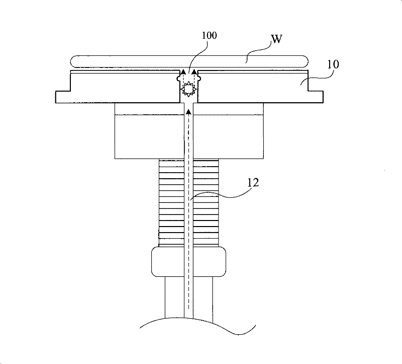
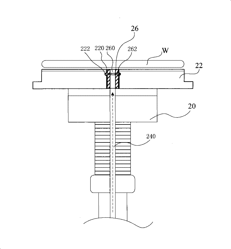
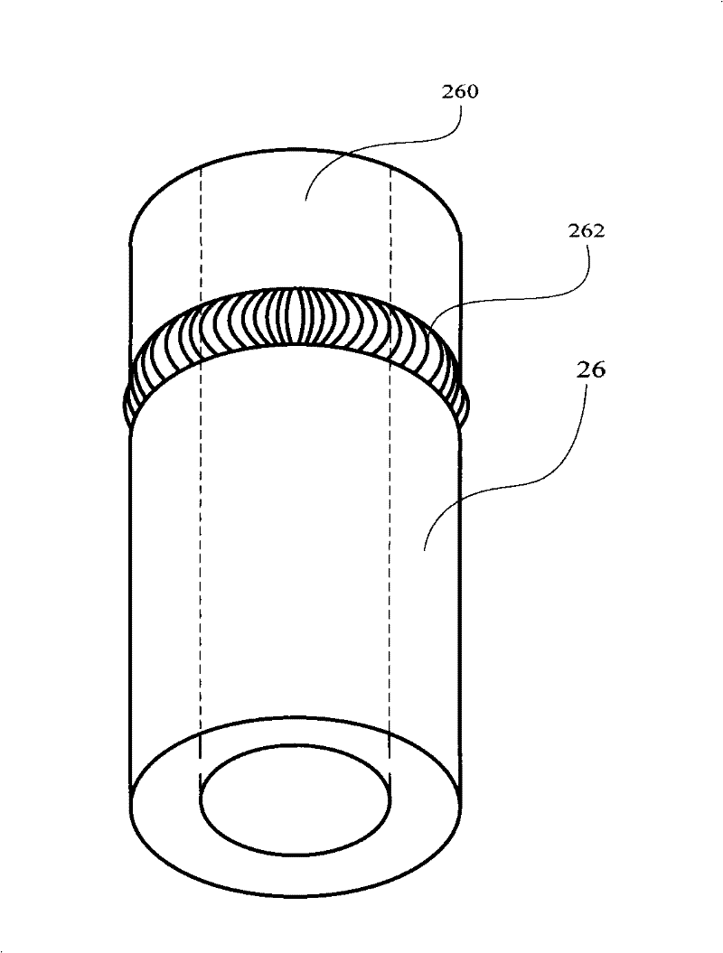
[0024] The present invention provides a wafer carrying device applied to semiconductor manufacturing process, comprising a carrying table with a central opening and a fluid pipeline corresponding to the central opening of the carrying table, wherein a shielding with a passage is also provided in the central opening of the carrying table components, and the passage communicates with the fluid pipeline. The shielding member can isolate the fluid in the passage from the radio-frequency electric energy, and prevent the fluid from generating an arc effect due to the action of the radio-frequency electric energy.

[0025] Embodiments of the present invention will be described below with reference to the accompanying drawings.

[0026] figure 2 It is a longitudinal sectional side view of the wafer carrying device in the first embodiment of the present invention. Such as figure 2 As shown, the wafer carrying device 2 is applied in an airtight processing container (not shown) for ...


PUM


Abstract

The invention discloses a wafer bearing device, which comprises a bearing platform provided with a central opening and a shielding piece, wherein the shielding piece is arranged in the central opening of the bearing platform and provided with an access. Since the shielding piece is arranged in the central opening of the bearing platform, the radio-frequency current and fluid in a fluid pipeline are mutually isolated by the shielding piece, the phenomenon that an electric arc mark is formed through an electric arc effect due to a conductive plasma generated by the fluid caused by being subjectto the radio-frequency electric energy action in the semiconductor production process can be avoided, the damage to a wafer and the bearing platform can be reduced, the service life of the wafer bearing device can be prolonged and the yield of products can be correspondingly improved.

Description

technical field [0001] The invention relates to a wafer carrying device. Background technique [0002] Generally, during the processing of semiconductor wafers, such as physical vapor deposition (PVD) or chemical vapor deposition (CVD), the reaction is carried out in a certain closed chamber. [0003] Taking the PVD process as an example, it is generally carried out in a processing device capable of generating plasma. Such a processing device has a reaction chamber in which a carrying device for holding a wafer to be processed is arranged. [0004] figure 1 To show a longitudinal sectional side view of an existing PVD device. Such as figure 1 As shown, the PVD device includes a carrier 10 having a central opening 100 and a fluid pipeline 12 corresponding to the central opening 100 of the carrier 10 . The carrier 10 can be, for example, an electrostatic chuck (E-Chuck), which has a suction function when it is connected with a radio frequency generator (RFPower) and gener...

Claims


Application Information

Patent Timeline
Patent Type & Authority Patents(China)
IPC IPC(8): H01L21/683C23C14/50C23C16/458C30B25/12
Inventor 周华邢程吴侃
Owner SEMICON MFG INT (SHANGHAI) CORP
Features
  • Generate Ideas
  • Intellectual Property
  • Life Sciences
  • Materials
  • Tech Scout
  • Unparalleled Data Quality
  • Higher Quality Content
  • 60% Fewer Hallucinations
Learn More