Display substrate, display panel and display device

A display substrate and display panel technology, applied in the direction of instruments, electrical components, circuits, etc., can solve the problems of light loss, low display brightness, poor refractive index, etc., to reduce the difference of refractive index, improve display brightness, and reduce loss Effect

Active Publication Date: 2014-09-24
BOE TECH GRP CO LTD
View PDF6 Cites 26 Cited by
  • Summary
  • Abstract
  • Description
  • Claims
  • Application Information

AI Technical Summary

Problems solved by technology

[0003] At present, both OLED and LCD generally have the problem of low display brightness. This is because the anode in OLED and the pixel electrode and common electrode in LCD are generally made of indium tin oxide (ITO, Indium Tin Oxides) with a refractive index of 1.8. There is a large refractive index difference between the ITO film and the glass substrate with a refractive index of 1.5. When the incident light passes through the ITO film and then hits the glass substrate, part of the incident light will be totally reflected. In this way, from the glass substrate There will be a problem of loss of light emitted at the place, which directly affects the display brightness of OLED and LCD

Method used


Image

  • Display substrate, display panel and display device
  • Display substrate, display panel and display device
  • Display substrate, display panel and display device

Examples


Embodiment Construction

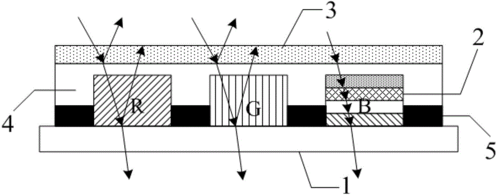
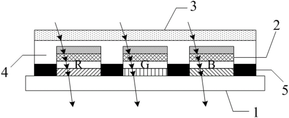
[0022] The specific implementation manners of the display substrate, the display panel and the display device provided by the embodiments of the present invention will be described in detail below with reference to the accompanying drawings.

[0023] The shape and thickness of each film layer in the accompanying drawings do not reflect their true proportions, and the purpose is only to illustrate the content of the present invention.

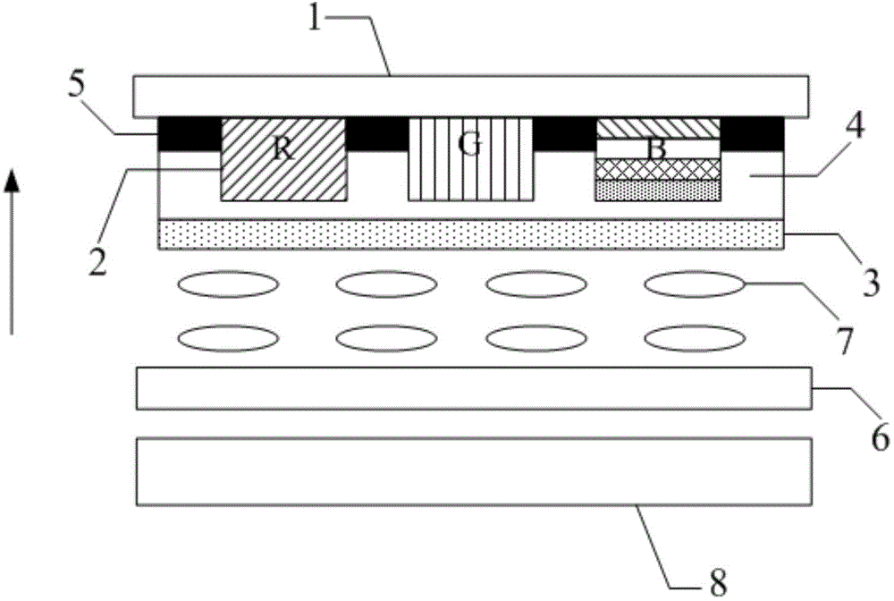
[0024] A display substrate provided by an embodiment of the present invention, such as Figure 1a and Figure 1b As shown, it includes: a base substrate 1, and a color filter structure 2 and a transparent conductive oxide film layer 3 sequentially stacked on the base substrate 1; the color filter structure 2 includes a plurality of color resists arranged in a matrix with different colors (like Figure 1a and Figure 1b The colors shown are three color resists of red (R), green (G) and blue (B) respectively);

[0025] The color resistance of at...


PUM

PropertyMeasurementUnit
thicknessaaaaaaaaaa
thicknessaaaaaaaaaa
refractive indexaaaaaaaaaa

Abstract

The invention discloses a display substrate, a display panel and a display device. Since the color resistance of at least one color in a colorful-film structure of the display substrate consists of at least two layers of light-filtering films which are arranged in a laminating manner; in the color resistance consisting of at least two layers of light-filtering films, the refractive indexes of all the light-filtering films are increased gradually along the direction from a substrate base plate to a transparent conductive oxide film layer, and the refractive index of one layer of light-filtering film adjacent to the substrate base plate is greater than the refractive rate of the substrate base plate, and one layer of light-filtering film adjacent to the transparent conductive oxide film layer is less than the refractive index of the transparent conductive oxide film layer. Therefore, the display substrate, the display panel and the display device have the advantages that in the process that light enters from the transparent conductive oxide film layer, passes through the colorful-film structure and then exits from the substrate base plate, the full-reflection phenomenon caused by larger refractive-rate difference between the transparent conductive oxide film layer and the substrate base plate can be reduced, so that the loss of the light in the transporting process of the display panel can be reduced and further the display brightness of the display device can be increased.

Description

technical field [0001] The present invention relates to the field of display technology, in particular to a display substrate, a display panel and a display device. Background technique [0002] Among existing display devices, organic electroluminescent display devices (OLED, Organic Light Emitting Diode) have the advantages of simple preparation process, low cost, high luminous efficiency, and easy formation of flexible structures; liquid crystal display devices (LCD, Liquid Crystal Display) It has the advantages of low power consumption, high display quality, no electromagnetic radiation, and wide application range. Organic electroluminescent display devices and liquid crystal display devices are relatively important display devices at present. [0003] At present, both OLED and LCD generally have the problem of low display brightness. This is because the anode in OLED and the pixel electrode and common electrode in LCD are generally made of indium tin oxide (ITO, Indium ...

Claims


Application Information

Patent Timeline
Patent Type & Authority Applications(China)
IPC IPC(8): G02F1/1335H01L27/32H01L51/52
CPCG02B5/201G02F2203/026G02F1/133514H10K59/35H10K59/38H10K50/858H10K50/80H10K50/816H10K50/828H10K50/841H10K59/00G02F1/1335G02F1/133512G02F2202/16
Inventor 焦志强孙力
Owner BOE TECH GRP CO LTD
Why Eureka
Try Eureka