Chemical Mechanical Polishing Method and Chip Layout Equivalent Feature Parameter Extraction Method

A technology of feature parameters and extraction methods, applied in special data processing applications, electrical digital data processing, instruments, etc., can solve the problems of low yield and low precision of integrated circuits, and achieve high yield and precision. low effect

Active Publication Date: 2017-02-15
INST OF MICROELECTRONICS CHINESE ACAD OF SCI
View PDF5 Cites 0 Cited by
  • Summary
  • Abstract
  • Description
  • Claims
  • Application Information

AI Technical Summary

Problems solved by technology

[0007] However, in the prior art, the method of using the CMP model to predict the surface topography of the chip has low precision, resulting in a low yield rate of the integrated circuit

Method used


Image

  • Chemical Mechanical Polishing Method and Chip Layout Equivalent Feature Parameter Extraction Method
  • Chemical Mechanical Polishing Method and Chip Layout Equivalent Feature Parameter Extraction Method
  • Chemical Mechanical Polishing Method and Chip Layout Equivalent Feature Parameter Extraction Method

Examples


Embodiment Construction

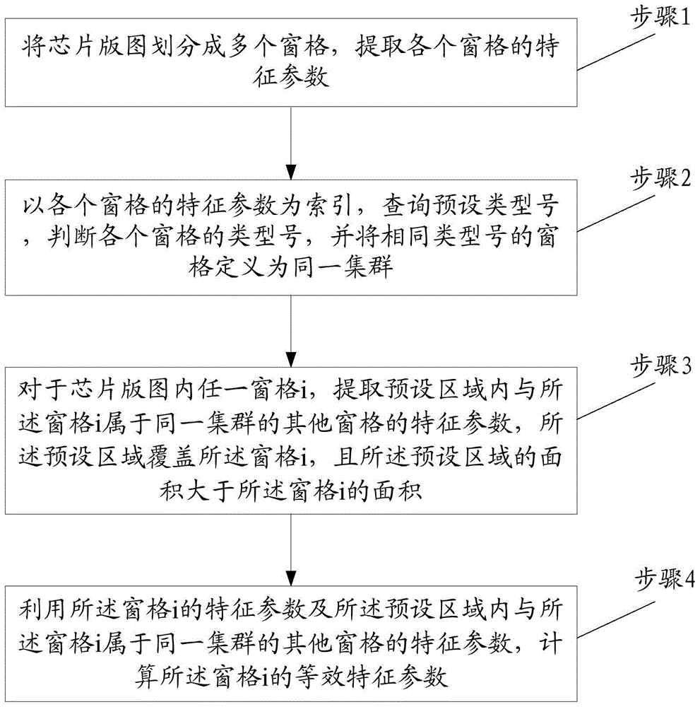
[0042] As mentioned in the background art section, in the prior art, the method for predicting chip surface topography using a CMP model has low accuracy, resulting in a low yield rate of integrated circuits.

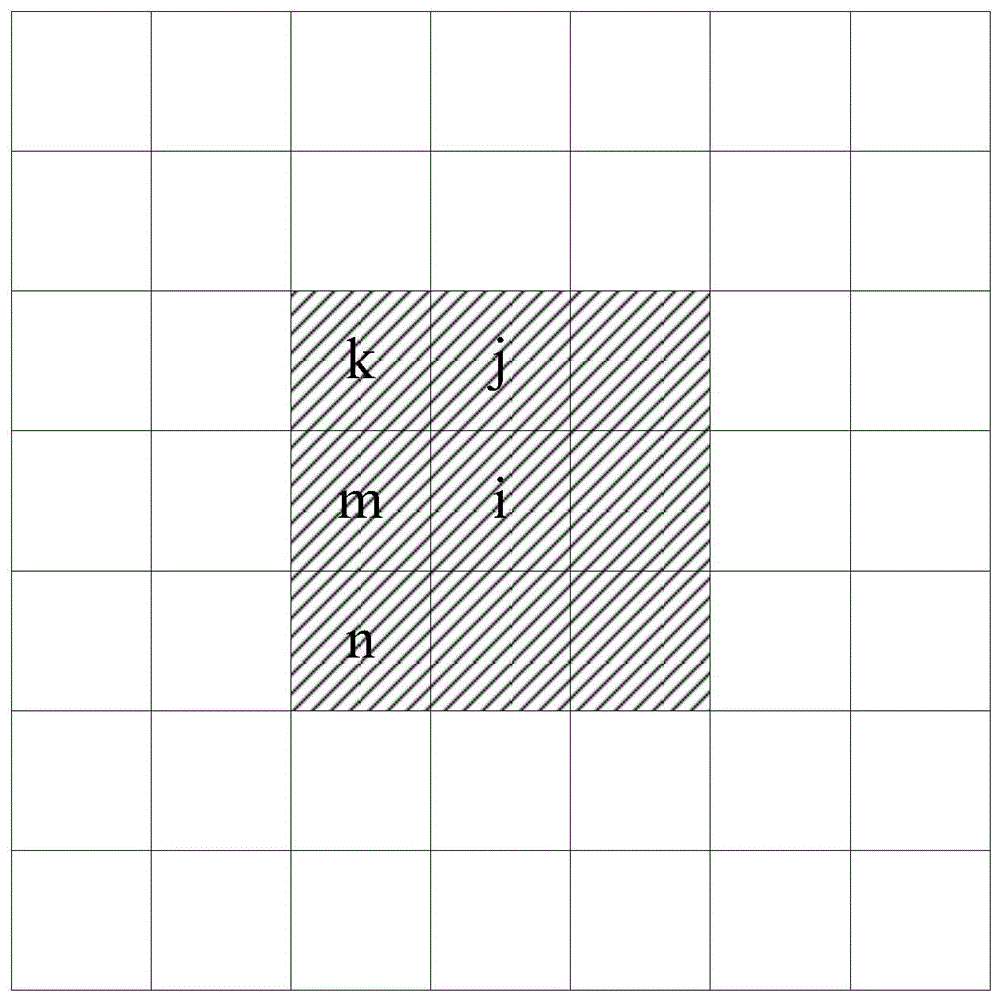
[0043] In the CMP simulation process, layout division and feature parameter extraction are very important steps. All subsequent simulation processes are based on the divided panes and the extracted feature parameters. Different layout division methods and different feature parameter extraction method, will lead to different CMP simulation results. If an unreasonable layout division method and characteristic parameter extraction method are adopted, the complexity of the subsequent CMP simulation process will be increased and the accuracy of the CMP simulation results will be reduced.

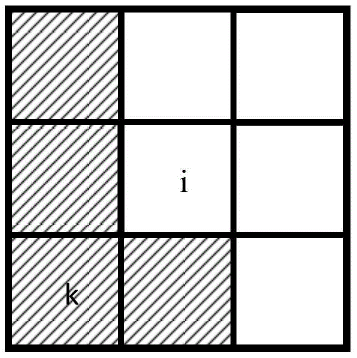
[0044]The method of layout division and feature parameter extraction in the prior art is as follows: first, starting from the starting point of the layout, using a fixed-size pane (or slig...


PUM


Abstract

The invention discloses a chemically mechanical polishing method and an extracting method for a chip layout equivalent characteristic parameter. The extracting method comprises the following steps: partitioning a chip layout into a plurality of window lattices, and extracting the characteristic parameter of each window lattice; taking the characteristic parameter of each window lattice as an index, inquiring pre-arranged category numbers, judging the category number of each window lattice, and defining the window lattices with a same category number as a same cluster; to any window lattice i in the chip layout, extracting characteristic parameters of other window lattices which belong to a same cluster with the window lattice i in a pre-arranged area, wherein the pre-arranged area covers the window lattice i, and the area of the pre-arranged area is greater than the area of the window lattice i; calculating the equivalent characteristic parameter of the window lattice i by adopting the characteristic parameter of the window lattice i and the characteristic parameters of other window lattices which belong to the same cluster with the window lattice i in the pre-arranged area. Precision of the method that adopting the CMP model to forecast the surface appearance of a chip is improved; yield of an integrated circuit is improved.

Description

technical field [0001] The invention relates to the technical field of chemical mechanical polishing, in particular to a method for extracting equivalent characteristic parameters of a chip layout, and a chemical mechanical polishing method including the method for extracting equivalent characteristic parameters of a chip layout. Background technique [0002] In the manufacturing process of integrated circuits (Integrated Circuit, IC), metals, dielectrics and other materials are applied to the surface of silicon wafers by various methods such as physical vapor deposition and chemical vapor deposition, so that A layered metal structure is formed. An integrated circuit usually includes a multilayer metal structure, and a dielectric layer is formed between adjacent layer metal structures, and the metal structures of different layers are connected through a plurality of metal-filled via holes, so that the multilayer metal structures in the integrated circuit The structures are ...

Claims


Application Information

Patent Timeline
Patent Type & Authority Patents(China)
IPC IPC(8): G06F17/50G06F9/455G06F17/30
Inventor 陈岚马天宇孙艳
Owner INST OF MICROELECTRONICS CHINESE ACAD OF SCI
Why Eureka
Try Eureka