A method for preparing a pattern and a method for preparing a display substrate

A pattern and substrate technology, applied in semiconductor/solid-state device manufacturing, semiconductor devices, electrical components, etc., can solve the problem of low pattern accuracy and achieve the effect of ensuring accuracy

Active Publication Date: 2021-12-28
BOE TECH GRP CO LTD
View PDF7 Cites 0 Cited by
  • Summary
  • Abstract
  • Description
  • Claims
  • Application Information

AI Technical Summary

Problems solved by technology

[0004] Embodiments of the present invention provide a method for preparing a pattern and a method for preparing a display substrate, which can solve the problem of low precision of patterns deposited by FMM

Method used


Image

  • A method for preparing a pattern and a method for preparing a display substrate
  • A method for preparing a pattern and a method for preparing a display substrate
  • A method for preparing a pattern and a method for preparing a display substrate

Examples


Embodiment Construction

[0034] The following will clearly and completely describe the technical solutions in the embodiments of the present invention with reference to the accompanying drawings in the embodiments of the present invention. Obviously, the described embodiments are only some, not all, embodiments of the present invention. Based on the embodiments of the present invention, all other embodiments obtained by persons of ordinary skill in the art without making creative efforts belong to the protection scope of the present invention.

[0035] An embodiment of the present invention provides a method for preparing a pattern, such as figure 1 shown, including:

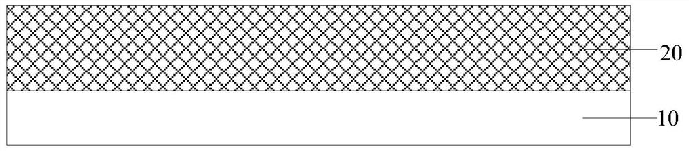
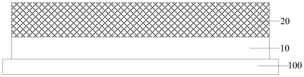
[0036] S100, such as figure 2 with image 3 As shown, the thermal insulation layer 20 is formed on the thermally conductive substrate 10 ;

[0037] Here, the heat insulating layer 20 may be formed on the heat conducting substrate 10 by methods such as deposition or coating.

[0038] In some embodiments, such as figure 2 As shown,...


PUM

PropertyMeasurementUnit
thicknessaaaaaaaaaa

Abstract

Embodiments of the present invention provide a method for preparing a pattern and a method for preparing a display substrate, which relate to the field of display technology and can solve the problem of low precision of patterns evaporated by FMM. The pattern preparation method includes forming a heat-insulating layer on a heat-conducting substrate; the thermal conductivity of the heat-conducting substrate is greater than that of the heat-insulating layer; patterning the heat-insulating layer to form a heat-insulating pattern; the heat-insulating pattern includes a hollow area; Form an evaporation material layer on one side of the heat-conducting substrate; face the surface of the target substrate to be patterned towards the evaporation material layer, and make the area to be patterned on the target substrate face the hollowed-out area of ​​the heat-insulating pattern; heat the heat-conducting substrate To the first temperature, the first temperature is greater than or equal to the evaporation temperature of the evaporation material layer; the evaporation material located in the hollow area in the evaporation material layer evaporates to the area to be patterned on the target substrate to form a pattern on the target substrate area forms a pattern.

Description

technical field [0001] The invention relates to the field of display technology, in particular to a method for preparing a pattern and a method for preparing a display substrate. Background technique [0002] At present, it is often necessary to use FMM (Fine Metal Mask, fine metal mask) to vapor-deposit patterns in the manufacturing process of the display device. For example, in the preparation of an OLED (Organic Light Emitting Diode, organic electroluminescent diode) display device, it is necessary to use FMM to vapor-deposit red light emitting patterns, green light emitting patterns and blue light emitting patterns. [0003] However, FMM is only suitable for preparing patterns in small and medium-sized display devices. For large-sized display devices, since the FMM will sag, the precision of the formed pattern will be low. In addition, for micro display devices and high PPI (Pixels Per Inch, pixel density) display devices, since the size of each sub-pixel is very small,...

Claims


Application Information

Patent Timeline
Patent Type & Authority Patents(China)
IPC IPC(8): H01L27/32H01L51/56H01L21/683
CPCH01L21/6835H01L2221/6835H10K59/122H10K71/80H10K59/1201H10K71/00
Inventor 张粲
Owner BOE TECH GRP CO LTD
Why Eureka
Try Eureka