Method for extracting chip layout features, cmp simulation method and system

A simulation method and layout technology, applied in design optimization/simulation, CAD circuit design, special data processing applications, etc., can solve problems such as reducing the accuracy of CMP simulation results, low integrated circuit yield, and graphic feature deviation, so as to reduce errors CMP hotspot information, shortening the production cycle, and improving the effect of precision

Active Publication Date: 2020-06-30
SEMICON MFG INT (SHANGHAI) CORP +1
View PDF8 Cites 0 Cited by
  • Summary
  • Abstract
  • Description
  • Claims
  • Application Information

AI Technical Summary

Problems solved by technology

However, in the above-mentioned prior art, when feature extraction is performed on the graphics in each divided pane, there is a deviation when identifying the current pane, such as figure 1 The current pane 10 (20nmx20nm or 10nmx10nm size) is graphically recognized as a dotted pane 11, and there is an offset, which causes a deviation in the graphic features extracted from the current pane 10, which affects the simulation results and reduces the accuracy of the CMP simulation results. accuracy, resulting in lower IC yields

Method used


Image

  • Method for extracting chip layout features, cmp simulation method and system
  • Method for extracting chip layout features, cmp simulation method and system
  • Method for extracting chip layout features, cmp simulation method and system

Examples


Embodiment Construction

[0055] In order to make the purpose and features of the present invention more obvious and understandable, the specific implementation of the present invention will be further described below in conjunction with the accompanying drawings. However, the present invention can be implemented in different forms and should not be limited to the described embodiments.

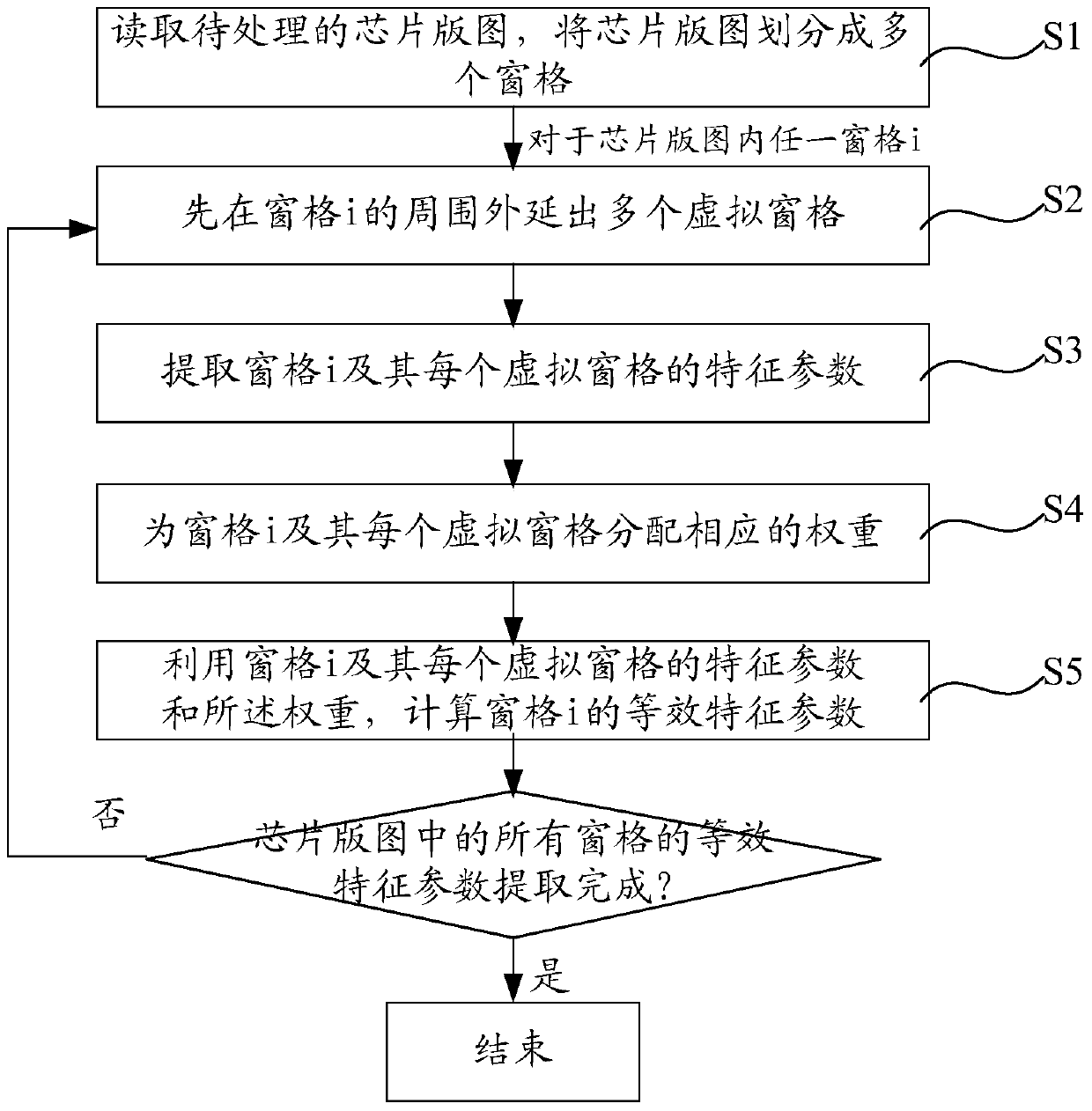
[0056] Please refer to figure 2 , the present invention proposes a method for extracting chip layout features, including:

[0057] S1, read the chip layout to be processed, and divide the chip layout into multiple panes;

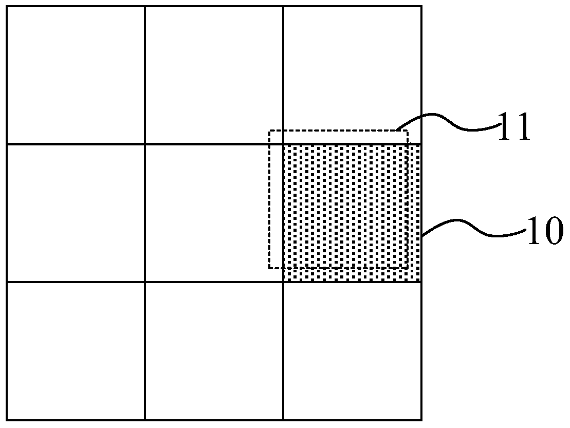
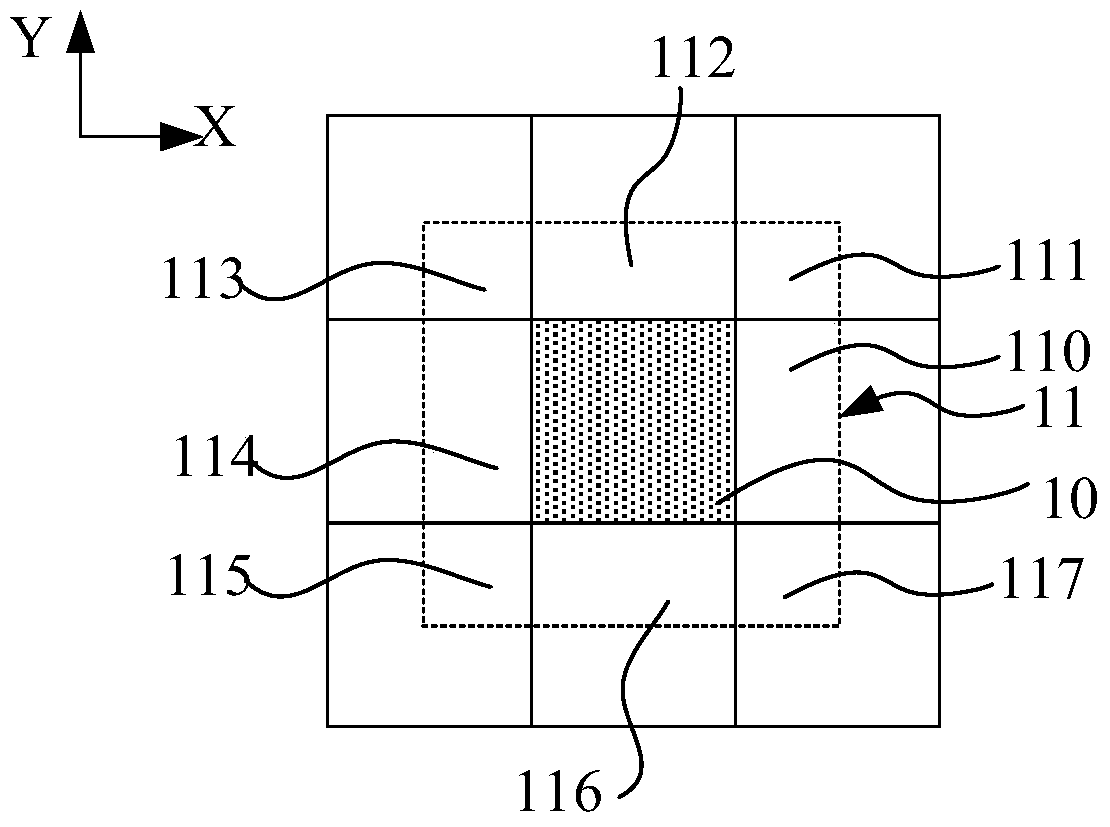
[0058] S2. For any pane in the chip layout, first extend a plurality of virtual panes around the pane;

[0059] S3, extracting the feature parameters of the pane and each virtual pane;

[0060] S4, assigning corresponding weights to the pane and each virtual pane;

[0061] S5. Calculate an equivalent feature parameter of the pane by using the feature parameter of the pane and each virtual pane a...


PUM


Abstract

The invention provides a chip layout feature extraction method and a CMP simulation method and system. When equivalent feature parameter extraction is carried out on panes divided by a chip layout, the proximity effect among the panes of the chip layout in a CMP process is fully considered, a plurality of virtual panes around each pane extend from the pane in the chip layout, and weighted averaging is carried out on graphic feature parameters in the virtual pane area extending from each pane and graphic feature parameters of the pane, so that the extraction precision of equivalent feature parameters of each pane is improved, the correct prediction for the surface appearance of the chip layout is realized, the correctness of CMP process simulation is improved, the efficiency is relatively high, the research and development costs of an integrated circuit are reduced, and the yield of the integrated circuit is ensured.

Description

technical field [0001] The invention relates to the technical field of integrated circuit design, in particular to a method for extracting chip layout features, a CMP simulation method and a system. Background technique [0002] For more than half a century, the integrated circuit industry has developed rapidly. Following Moore's Law, the integration density of transistors on a wafer doubles every 18 months, and the corresponding device feature size is simultaneously reduced to 0.7 times. Technology nodes have reached 65nm, 45nm, and even 32nm, 23nm. However, with the continuous shrinking of the feature size of integrated circuits, there are more and more factors affecting chip performance and production yield in the production process. become more prominent. An ideal wafer surface is a prerequisite for smooth lithography. Chemical Mechanical Polishing (CMP, or chemical mechanical planarization) technology is used to planarize the wafer surface in the current VLSI stage. ...

Claims


Application Information

Patent Timeline
Patent Type & Authority Patents(China)
IPC IPC(8): G06F30/33G06F30/392
CPCG06F30/20G06F30/392
Inventor 李雪
Owner SEMICON MFG INT (SHANGHAI) CORP
Why Eureka
Try Eureka