Wafer purifying chamber for improving defect of coagulation of etching by-products

A technology for purifying chambers and by-products, used in electrical components, semiconductor/solid-state device manufacturing, circuits, etc., to ensure productivity, device stability and product yield improvement, and eliminate condensation defects.

Inactive Publication Date: 2014-10-01
SHANGHAI HUALI MICROELECTRONICS CORP
View PDF3 Cites 5 Cited by
  • Summary
  • Abstract
  • Description
  • Claims
  • Application Information

AI Technical Summary

Problems solved by technology

Therefore, the above methods have great disadvantages

Method used


Image

  • Wafer purifying chamber for improving defect of coagulation of etching by-products
  • Wafer purifying chamber for improving defect of coagulation of etching by-products

Examples


Embodiment Construction

[0025] The specific embodiment of the present invention will be further described in detail below in conjunction with the accompanying drawings.

[0026] It should be noted that, in the following examples, when describing the embodiments of the present invention in detail, in order to clearly show the structure of the present invention for the convenience of description, the structures in the drawings are not drawn according to the general scale, and the Partial enlargement, deformation and omission of processing should be avoided as a limitation of the present invention.

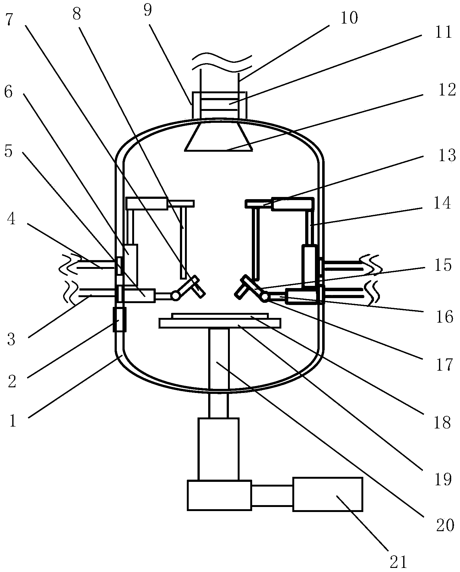
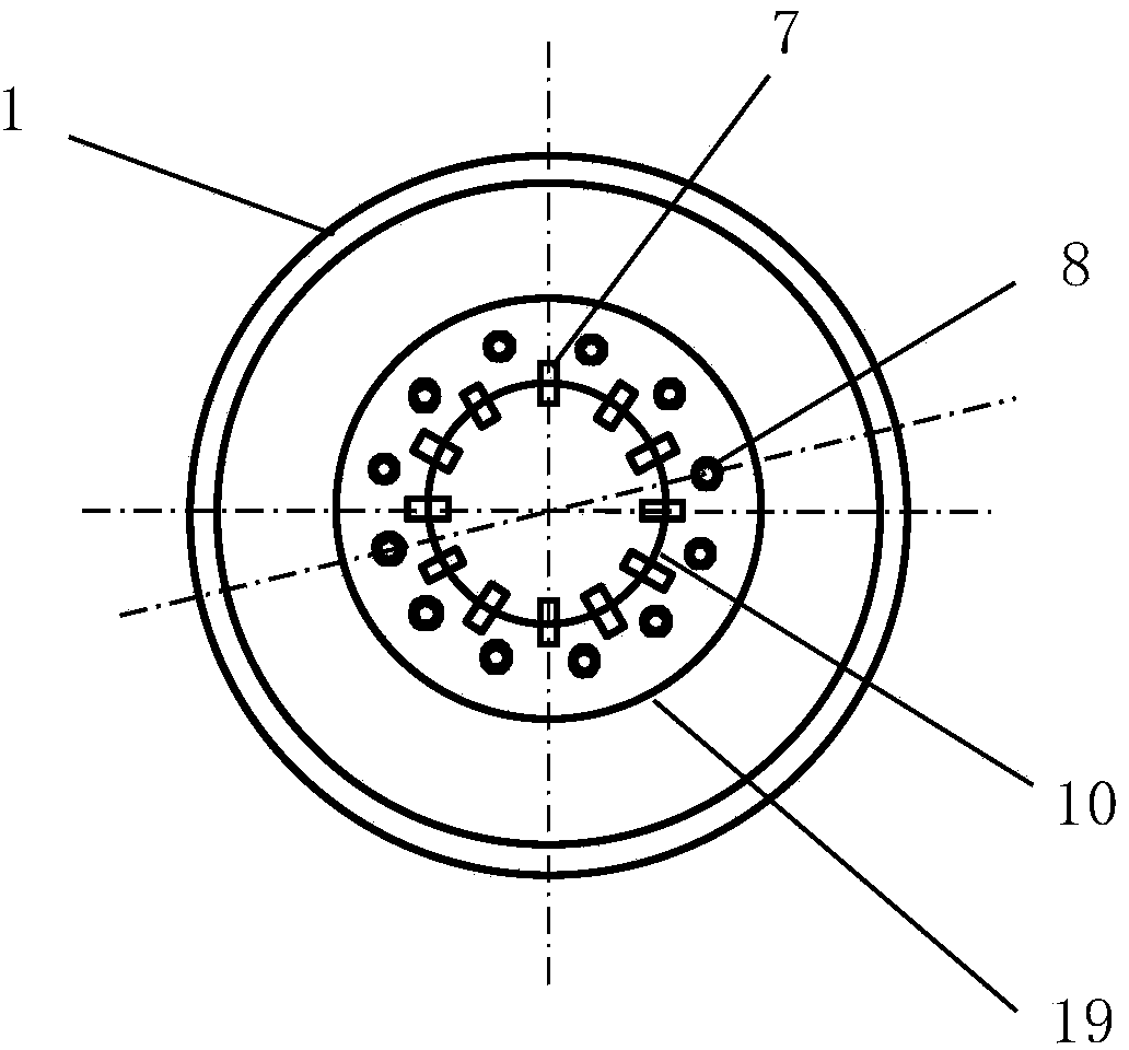
[0027] In this example, see figure 1 , figure 1 It is a structural schematic diagram of a wafer clean chamber for improving condensation defects of etching by-products according to the present invention. The wafer cleaning chamber of the present invention includes several components including a chamber body, a spray gun system, a wafer support platform system and an air extraction system. like figure 1 ...


PUM


Abstract

The invention discloses a wafer purifying chamber for improving the defect of coagulation of etching by-products. The wafer purifying chamber is used for conducting pre-purification treatment on a wafer after the wafer is etched and before the wafer is washed; purifying gas can be jetted simultaneously to the wafer in different directions at adjustable angles and distances through a plurality of top jetting guns and a plurality of side-wall jetting guns, which are arranged in the chamber body of the wafer purifying chamber and around the vertical center of the chamber body; used gas in the chamber body and etching by-products carried by the used gas are exhausted through an exhaust pipe at the top of the chamber body. Through the application of the wafer purifying chamber provided by the invention, not only can damage to the wafer, especially to a CD, be avoided, but also the etching by-products attached to the wafer can be avoided, so that the defect of coagulum produced by reaction of the etching by-products and water in a cleaning waiting process is eliminated.

Description

technical field [0001] The invention relates to a device for purifying a semiconductor wafer, and more particularly, to a wafer cleaning chamber for improving condensation defects generated by by-products of an etching process. Background technique [0002] With the development of integrated circuit technology and the scaling down of critical dimensions, the process windows of various processes are getting smaller and smaller, such as the depth, dose and even shape of ion implantation, etc. For example, the abnormal ion implantation shape of 55nm logic products Otherwise, it will lead to the failure of the final device or even the yield rate, resulting in loss. The abnormal morphology of ion implantation is often due to the residual by-products of polysilicon sidewall etching, the long waiting time in the cleaning process, and the condensation defects generated by the reaction with water in the air that block the normal ion implantation. Another example is the residue of by...

Claims


Application Information

Patent Timeline
Patent Type & Authority Applications(China)
IPC IPC(8): H01L21/67
CPCH01L21/67213H01L21/67161
Inventor 范荣伟陈宏璘龙吟顾晓芳郭浩
Owner SHANGHAI HUALI MICROELECTRONICS CORP
Why Eureka
Try Eureka