Color film substrate, manufacturing method thereof, display panel and display device

A technology of color film substrate and manufacturing method, which is applied in the directions of optics, instruments, electrical components, etc., can solve the problems of easy damage of cathode materials and ITO, and achieve the effects of avoiding uneven internal pressure, ensuring electrical conductivity, and reducing damage

Active Publication Date: 2014-10-01
BOE TECH GRP CO LTD
View PDF5 Cites 26 Cited by
  • Summary
  • Abstract
  • Description
  • Claims
  • Application Information

AI Technical Summary

Problems solved by technology

[0006] The invention provides a color filter substrate and its manufacturing method, a display panel and a display device to solve the technical problem that the cathode material and ITO are easily damaged after the medium-voltage box process in the prior art

Method used


Image

  • Color film substrate, manufacturing method thereof, display panel and display device
  • Color film substrate, manufacturing method thereof, display panel and display device
  • Color film substrate, manufacturing method thereof, display panel and display device

Examples


Embodiment Construction

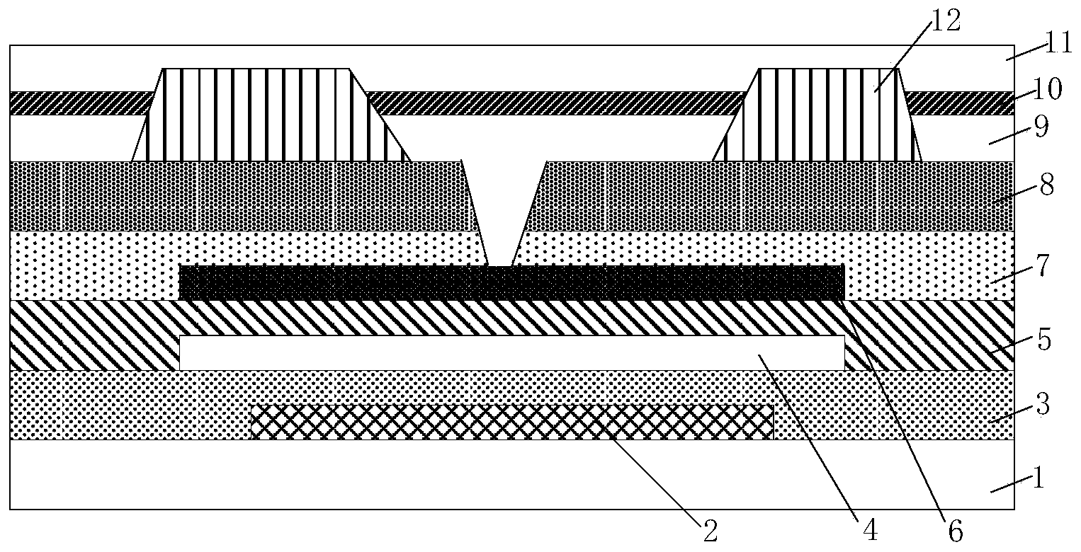
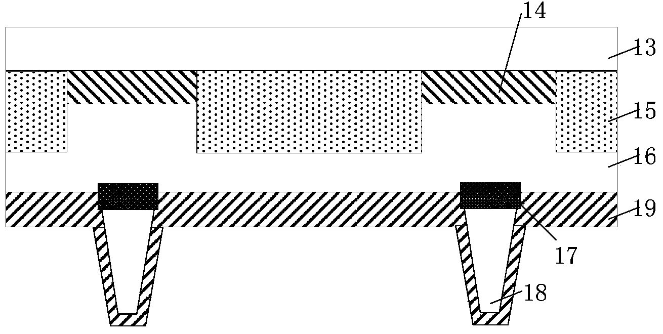
[0050] In order to make the purpose, technical solutions and advantages of the embodiments of the present invention clearer, the technical solutions in the embodiments of the present invention will be clearly and completely described below in conjunction with the drawings in the embodiments of the present invention. Obviously, the described embodiments It is a part of embodiments of the present invention, but not all embodiments. Based on the embodiments of the present invention, all other embodiments obtained by persons of ordinary skill in the art without creative efforts fall within the protection scope of the present invention.

[0051] In the drawing figures, the dimensions of layers and regions may be exaggerated for clarity of illustration. Also it will be understood that when an element or layer is referred to as being "on" another element or layer, it can be directly on the other element or intervening layers may be present. Further, it will be understood that when a...


PUM


Abstract

The invention provides a color film substrate, a manufacturing method of the color film substrate, a display panel and a display device. The color film substrate comprises a substrate body, single-layer color film layers and a color folding film layer, wherein the single-layer color film layers are formed on one side of the substrate body and located in color sub-pixel areas, and the color folding film layer is located between one part of the color sub-pixel areas and formed by multiple single-layer color film layers in a laminated mode. The color film substrate further comprises a shock insulator located between the other part of the color sub-pixel areas and an auxiliary electrode layer with which the surface of the color folding film layer is covered. The top surface of the shock insulator is higher than that of the color folding film layer, and the shock insulator can be elastically compressed in the height direction. The situation that the color film substrate cannot be used normally due to uneven internal pressure when a screen is oversize is avoided, the color film substrate is applied to display of OLEDs, damage to ITO materials and cathode materials of the auxiliary electrode layer can be effectively reduced, and a good electric conduction effect can be guaranteed.

Description

technical field [0001] The present invention relates to the field of display technology, in particular to a color filter substrate and a manufacturing method thereof, a display panel and a display device. Background technique [0002] At present, the white organic light-emitting diodes (WOLED) + color filter substrate (Color Filter, CF) technology adopts top-emitting electroluminescent (EL), has the advantages of high aperture ratio, and has been concerned by the industry. [0003] The basic structure of the WOLED array substrate in the prior art is as follows: figure 1 1 is the array substrate; 2 is the gate; 3 is the gate insulating layer; 4 is the active layer; 5 is the etch stop layer; 6 is the source and drain layer; 7 is the passivation layer; 8 is Resin insulating layer; 9 is a pixel electrode (ITO) layer, where the pixel electrode layer is used as an anode; 10 is a luminescent material; 11 is a cathode material; 12 is a pixel defining layer. The basic structure of ...

Claims


Application Information

Patent Timeline
Patent Type & Authority Applications(China)
IPC IPC(8): H01L27/32
CPCG02F1/1335G02F1/1339G02F1/1343H10K59/00
Inventor 孙宏达王东方林俊仪方金钢
Owner BOE TECH GRP CO LTD
Why Eureka
Try Eureka