

Wafer purifying equipment for eliminating etching byproduct coagulation defect of connecting hole
A technology for purifying equipment and by-products, applied in the manufacture of electrical components, semiconductor/solid-state devices, circuits, etc., can solve problems such as difficult cleaning, impure removal of defects, and reduced productivity, achieving a large process window and eliminating condensation Defects, the effect of ensuring productivity
- Summary
- Abstract
- Description
- Claims
- Application Information
AI Technical Summary
Problems solved by technology
Method used
Image

Examples
Embodiment 1
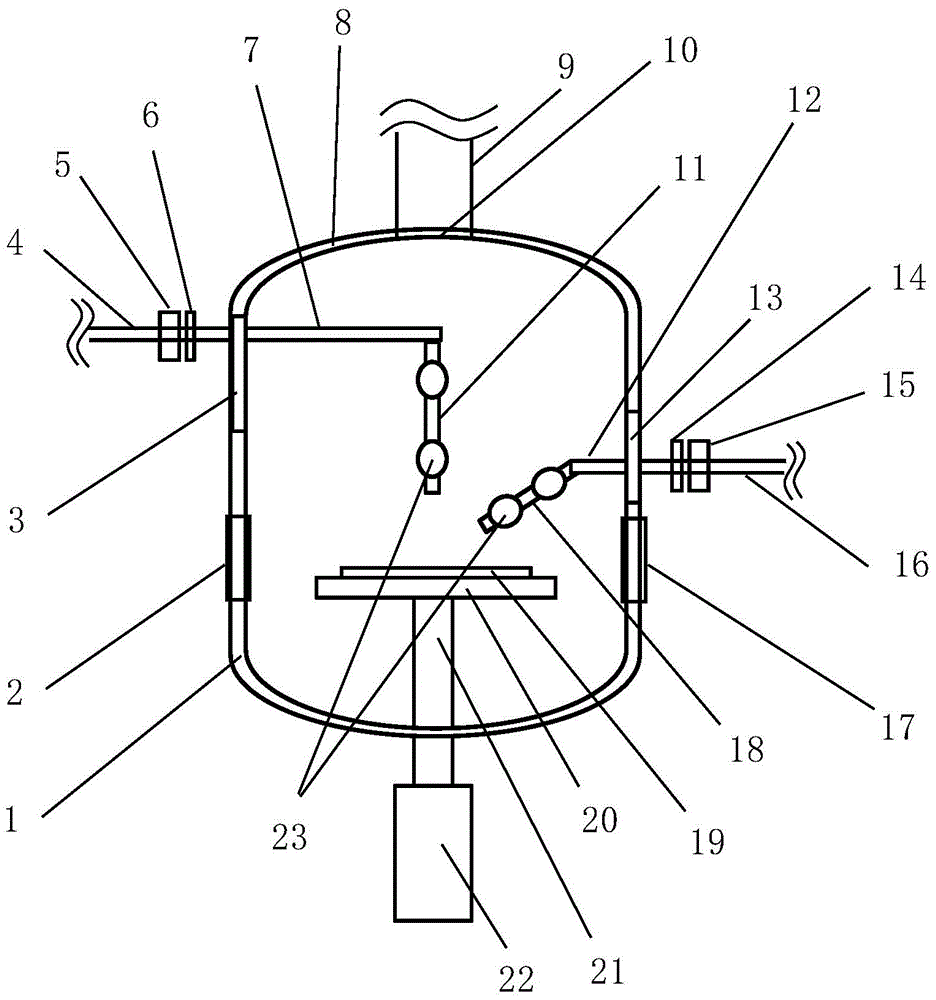
[0029] In this example, see figure 1 , figure 1 It is a structural schematic diagram of a wafer cleaning device for eliminating condensation defects of connection hole etching by-products according to the present invention. The wafer purification equipment of the present invention is used to perform pre-purification treatment on the wafer after the connection hole is etched and before the wafer is cleaned, so as to remove the etching by-products adhered to the wafer, so as to eliminate the etching by-products Condensation defects caused by reaction with water. The wafer purification equipment of the present invention includes several components including a cavity, a spray gun, a wafer support table and an exhaust pipe. Such as figure 1 As shown, the chamber 1 forms a closed space for cleaning the wafer 19 , and the chamber 1 has a dome-shaped upper inner wall 8 . Utilizing the guiding effect of the arc surface of the dome, the purified gas in the cavity 1 and the etching b...
Embodiment 2
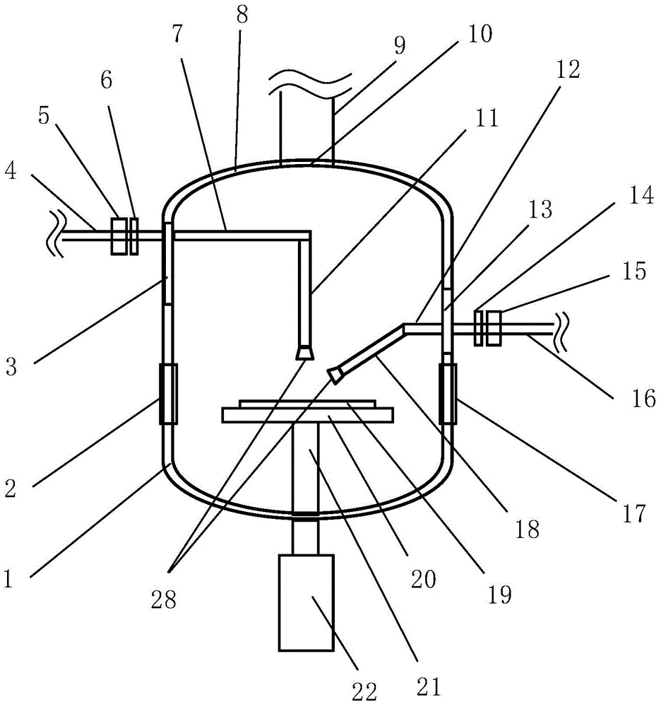
[0038] In this example, see image 3 , image 3 It is another structural schematic diagram of a wafer cleaning device for eliminating condensation defects of connection hole etching by-products of the present invention. Such as image 3 As shown, the main structure of the wafer cleaning equipment in this embodiment is exactly the same as in Embodiment 1, the only difference is that no gas agitation device is provided in the nozzles of the top spray gun 11 and the side wall spray gun 18, but in The injection ports of the top injection gun 11 and the side wall injection gun 18 are each provided with a nozzle 28, through which the injection form and outlet pressure of the purified gas can be adjusted. In this embodiment, the nozzle 28 adopts a shower-shaped spout (the spout is the same as a common shower, and the drawing is omitted). The shower-shaped nozzle can divide the purification gas into multiple bundles of pressurized jets to the wafer 19, while expanding the direct sc...
PUM
 Abstract
Description
Claims
Application Information