Array substrate manufacturing method

A technology of array substrate and photoresist, which is applied in the photoplate process of patterned surface, semiconductor/solid-state device manufacturing, instruments, etc., can solve the problem of reducing factory production capacity and product yield, low product efficiency, complex production process, etc. problem, to achieve the effect of improving product yield and product benefit, saving film forming and masking process, and reducing production cost

Inactive Publication Date: 2014-10-08
HEFEI XINSHENG OPTOELECTRONICS TECH CO LTD +1
View PDF5 Cites 15 Cited by
  • Summary
  • Abstract
  • Description
  • Claims
  • Application Information

AI Technical Summary

Problems solved by technology

[0004] The etch barrier metal oxide IGZO TFT has a simple manufacturing process, and the etch barrier layer on the metal oxide IGZO can protect the metal oxide IGZO layer from being damaged when the source and drain metal electrodes are formed, thereby improving the performance of the metal oxide IGZO TFT. Performance, but requires an additional photolithography process to form an etch barrier layer, inc

Method used


Image

  • Array substrate manufacturing method
  • Array substrate manufacturing method
  • Array substrate manufacturing method

Examples


Embodiment Construction

[0030] The specific implementation manners of the present invention will be further described in detail below in conjunction with the accompanying drawings and embodiments. The following examples are used to illustrate the present invention, but are not intended to limit the scope of the present invention.

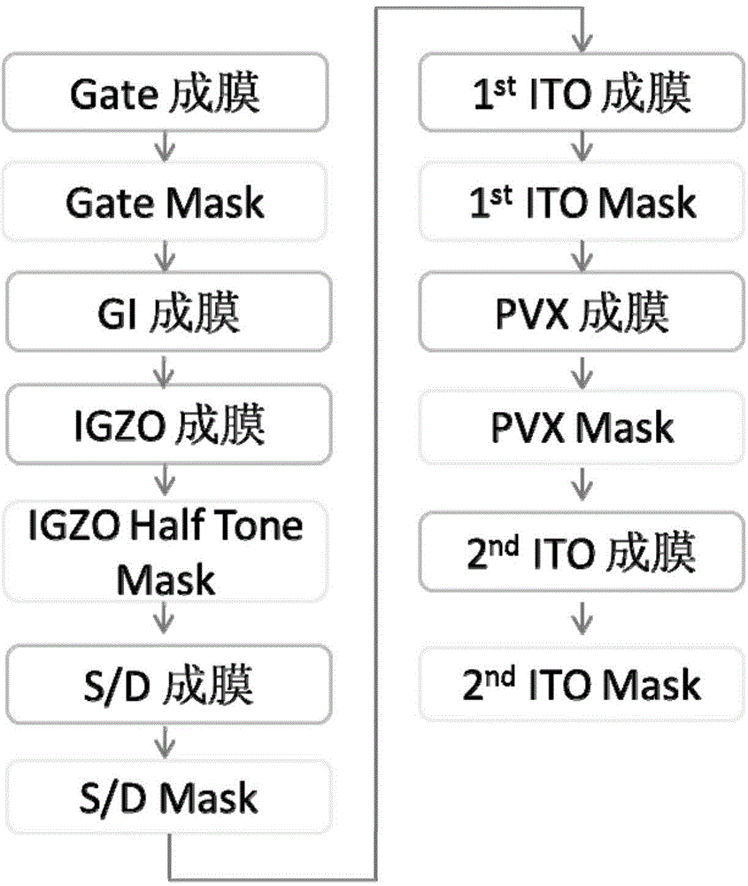
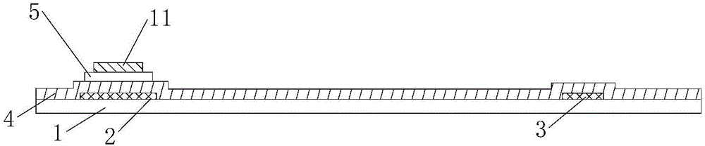
[0031] In order to simplify the production process of etch-stop TFT, reduce its production cost, and improve product yield and product benefit, the present invention provides an improved method for preparing an array substrate. Specifically, during the formation of the active layer, the Partial thickness of photoresist at the corresponding position of the channel region between the source and drain electrodes above the source layer; then form the source and drain metal layer, and further form the source and drain electrodes; The photoresist is stripped, so that the damage to the metal oxide layer is avoided in the etching process of the source-drain electrode formation pro...


PUM


Abstract

The invention discloses an array substrate manufacturing method. According to the method, in the active layer forming process, photoresist of partial thickness on the corresponding position of a channel region between the source drain electrodes above the active layer is reserved; then a source leakage metal layer is formed, and the source drain electrodes are further formed; finally the photoresist of partial thickness on the channel region between the source drain electrodes is stripped. According to the array substrate manufacturing method, when the semiconducting film is formed, partial photoresist is reserved on the TFT channel region through the semi-permeable mask process, damage to the metal oxide layer in the source leakage electrode etching process is avoided, the photoresist is stripped in the later stripping process, a traditional etching blocking layer can be replaced, the processes of film forming and masking for etching the blocking layer are omitted, production cost is reduced, the process is simplified, and product yield and product benefits are improved.

Description

technical field [0001] The present invention relates to the field of display technology, in particular to a method for preparing an array substrate. Background technique [0002] In recent years, with the continuous increase of the size of liquid crystal display and the continuous increase of the frequency of the driving circuit, the mobility of the existing amorphous silicon thin film transistor is difficult to meet the demand. The mobility of the amorphous silicon thin film transistor is generally around 0.5cmW·S. When the size of the liquid crystal display exceeds 80 inches and the driving frequency is 120 Hz, the mobility of more than 1 cmW·S is required. It is obviously difficult to meet the mobility of amorphous silicon. High-mobility thin film transistors are polysilicon thin film transistors and metal oxide thin film transistors. Although the research on polysilicon thin film transistors started relatively early, the uniformity of polysilicon thin film transistors is...

Claims


Application Information

Patent Timeline
IPC IPC(8): H01L21/77G03F1/32
CPCH01L27/1288H01L29/66969H01L27/1225H01L29/7869H01L27/127H01L29/495
Inventor 王凯
Owner HEFEI XINSHENG OPTOELECTRONICS TECH CO LTD
Why Eureka
Try Eureka