Semiconductor device and method for production of high avalanche energy LDMOS device

A semiconductor and device technology, applied in the field of semiconductor devices, can solve the problems of larger device size and higher cost, and achieve the effects of stable threshold voltage, low resistance and high avalanche energy

Active Publication Date: 2014-10-08
CHENGDU MONOLITHIC POWER SYST
View PDF6 Cites 3 Cited by
  • Summary
  • Abstract
  • Description
  • Claims
  • Application Information

AI Technical Summary

Problems solved by technology

However, these methods will increase the size of the device and greatly increase the cost

Method used


Image

  • Semiconductor device and method for production of high avalanche energy LDMOS device
  • Semiconductor device and method for production of high avalanche energy LDMOS device
  • Semiconductor device and method for production of high avalanche energy LDMOS device

Examples


Embodiment Construction

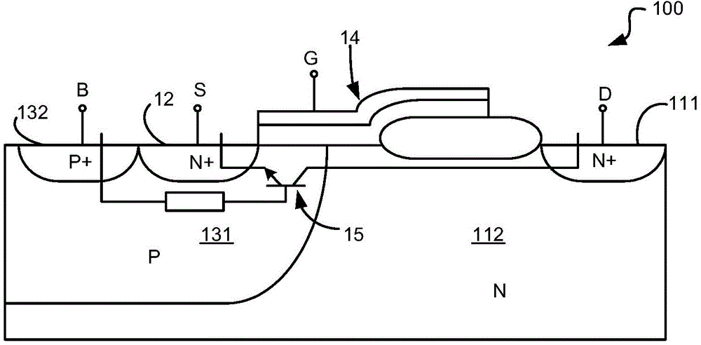
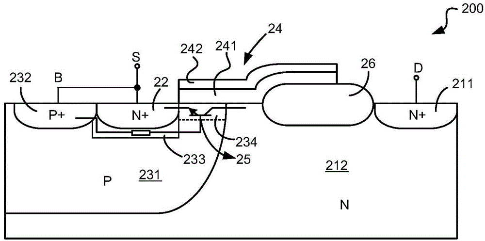
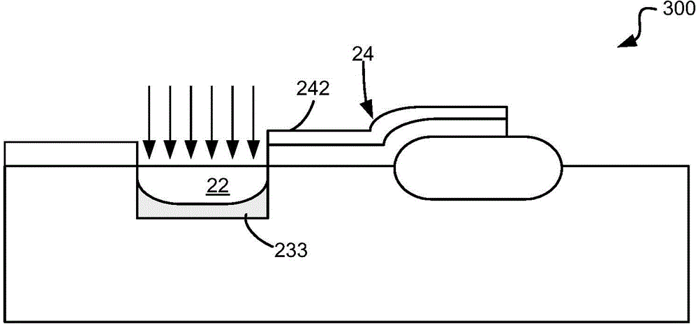
[0019] Specific embodiments of the present invention will be described in detail below, and it should be noted that the embodiments described here are only for illustration, not for limiting the present invention. In the following detailed description of the invention, numerous details are set forth in order to better understand the invention. However, it will be understood by those skilled in the art that the present invention may be practiced without these specific details. In order to clearly illustrate the present invention, detailed descriptions of some specific structures and functions are simplified herein. In addition, similar structures and functions that have been described in detail in some embodiments will not be repeated in other embodiments. Although terms of the present invention have been described in conjunction with specific exemplary embodiments, these terms should not be construed as being limited to the exemplary embodiments set forth herein.

[0020] Ac...


PUM


Abstract

The invention discloses a semiconductor device, an LDMOS device and a method for the production of a high avalanche energy LDMOS device. The semiconductor device includes a gate region, an N-type drain region, a P-type body region and an N-type source region, wherein the body region comprises a first body region, a second body region and a body contact region, wherein the first body region is doped with boron atoms, the second body region is doped with indium atoms and boron atoms, and the second body region is located beneath and adjacent to the source region. The semiconductor device, the LDMOS device and the method for the production of the high avalanche energy LDMOS device have the advantages of lower resistance, higher avalanche energy and stable threshold voltage and so on.

Description

technical field [0001] The present invention relates to a semiconductor device, specifically but not limited to an LDMOS device and a method for increasing its avalanche energy. Background technique [0002] figure 1 A cross-sectional view of a prior art laterally diffused metal oxide semiconductor field effect transistor (LDMOS) device 100 is shown. LDMOS device 100 includes a drain, a source, a body region and a gate 14 . The drain includes a drift region 112 and a drain contact region 111 . The source comprises a source region 12 . The body of the LDMOS includes a body region 131 and a body contact region 132 . In normal operation, a voltage is applied to the gate 14 and the drain of the LDMOS device 100, wherein the voltage on the gate 14 inverts the channel region under the gate 14 into the same conduction type as the drain and source , forming a current channel between the source 12 and the drain. When the voltage applied to the drain is too high to exceed the br...

Claims


Application Information

Patent Timeline
Patent Type & Authority Applications(China)
IPC IPC(8): H01L29/78H01L21/336
CPCH01L29/66681H01L29/0626H01L29/7816H01L29/1095H01L21/26513H01L29/36H01L29/42368H01L29/66689H01L29/0878H01L29/167H01L21/265H01L29/086H01L29/4916H01L29/51H01L29/66659H01L29/7835
Inventor 乔伊·迈克格雷格郑志星艾瑞克·布劳恩吉扬永
Owner CHENGDU MONOLITHIC POWER SYST
Why Eureka
Try Eureka