Vertical double-diffused metal oxide semiconductor device and fabrication method therefor

An oxide semiconductor and vertical double-diffusion technology, which is applied in semiconductor/solid-state device manufacturing, semiconductor devices, transistors, etc., can solve the problems of low avalanche energy of devices and easy opening of parasitic triodes, etc.

Active Publication Date: 2017-07-04
WUXI CHINA RESOURCES HUAJING MICROELECTRONICS
View PDF4 Cites 0 Cited by
  • Summary
  • Abstract
  • Description
  • Claims
  • Application Information

AI Technical Summary

Problems solved by technology

[0006] The invention provides a vertical double-diffused metal oxide semiconductor device and a manufacturing method thereof, so as to solve the problems in the prior art that the parasitic triode of the vertical double-diffused metal oxide semiconductor device is easy to turn on and the device has low avalanche energy

Method used


Image

  • Vertical double-diffused metal oxide semiconductor device and fabrication method therefor
  • Vertical double-diffused metal oxide semiconductor device and fabrication method therefor
  • Vertical double-diffused metal oxide semiconductor device and fabrication method therefor

Examples


Embodiment 1

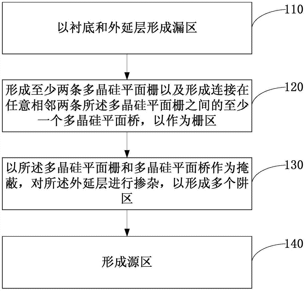
[0031] figure 2 It is a flow chart of a method for manufacturing a vertical double-diffused metal oxide semiconductor device provided in Embodiment 1 of the present invention. The method specifically includes the following steps:

[0032] Step 110, forming a drain region with the substrate and the epitaxial layer.

[0033] Taking an N-channel vertical double-diffused metal oxide semiconductor device as an example, an N-type epitaxial layer is fabricated on an N+ substrate, and the N+ type substrate and the N-type epitaxial layer are used as a drain region.

[0034] Step 120 , forming at least two polysilicon planar gates and forming at least one polysilicon planar bridge connected between any two adjacent polysilicon planar gates as gate regions.

[0035] Specifically, the polysilicon planar bridge includes two left and right strip structures connected to the polysilicon planar gate. Preferably, the center area of ​​the polysilicon planar bridge is strip-shaped, circular or ...

Embodiment 2

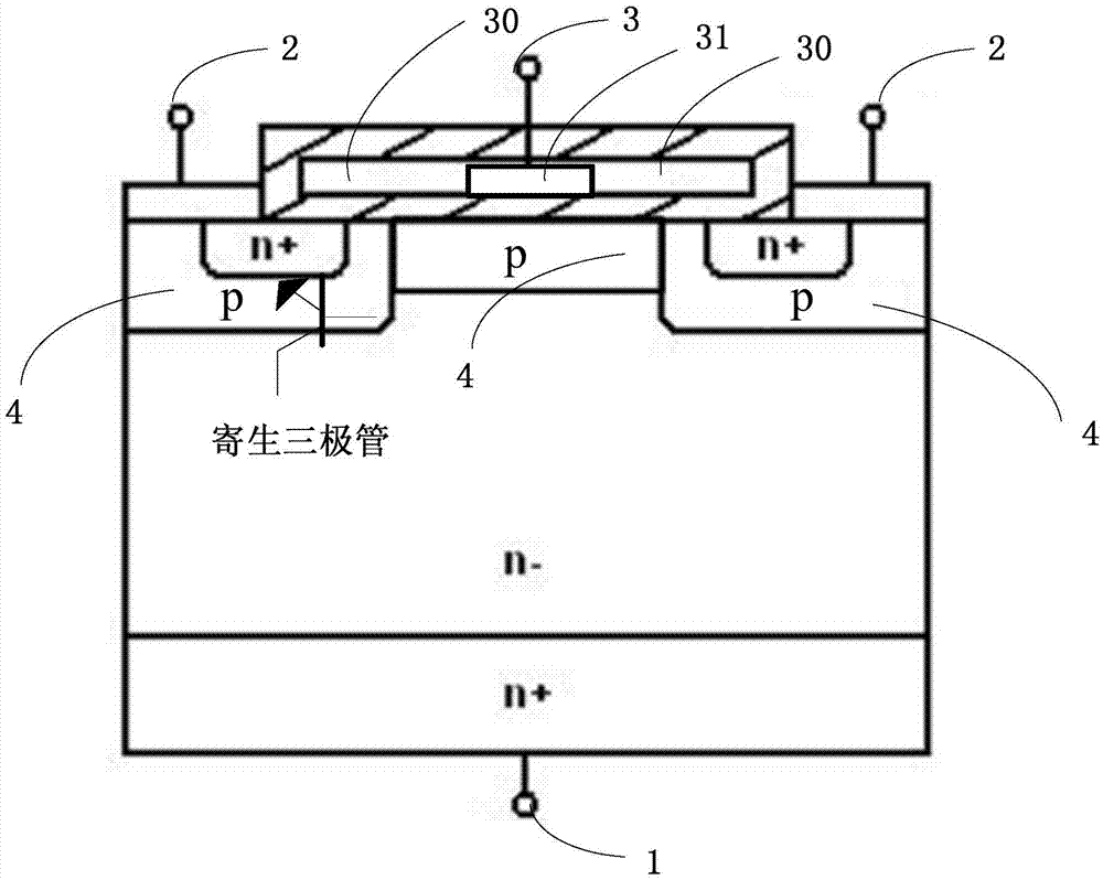
[0045] image 3 A schematic structural diagram of a vertical double-diffused metal-oxide-semiconductor device provided by Embodiment 2 of the present invention. The structure of the vertical double-diffused metal oxide semiconductor device includes: a drain region 1, a source region 2 and a gate region 3, and the gate region 3 includes:

[0046] At least two polysilicon planar gates 30, and at least one polysilicon planar bridge 31 connected between any adjacent two polysilicon planar gates.

[0047] Taking an N-channel vertical double-diffused metal oxide semiconductor device as an example, after the gate region 3 is formed, preferably, the vertical double-diffused metal oxide semiconductor device further includes: using the polysilicon planar gate 30 and the polysilicon planar bridge 31 as A plurality of well regions 4 formed after doping the epitaxial layer N- is masked, preferably, the well regions 4 are P well regions.

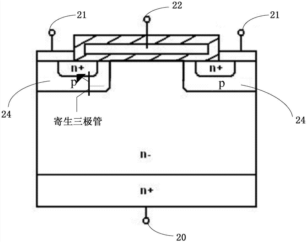
[0048] image 3 The parasitic triode is shown, b...


PUM


Abstract

The invention discloses a vertical double-diffused metal oxide semiconductor device and a fabrication method therefor. The fabrication method comprises the steps of forming a drain region based on a substrate and an epitaxial layer; forming at least two polysilicon plane gates and forming at least one polysilicon plane bridge connected between any adjacent two polysilicon plane gates to be used as a gate region; and by taking the polysilicon plane gates and the polysilicon plane bridge as shielding, performing doping on the epitaxial layer to form a plurality of well regions so as to form a source region. By virtue of the scheme, multiple well regions can be formed below the gate region; the well regions formed below the polysilicon plane bridge in the gate region are connected through diffusion; in addition, the well regions formed below the polysilicon plane bridge in the gate region are relatively shallow, so that a reverse current can flow through the multiple relatively-shallow well regions formed below the polysilicon plane bridge in the gate region easily when the vertical double-diffused metal oxide semiconductor device is in an avalanche state, so that the avalanche energy of the semiconductor device is improved.

Description

technical field [0001] Embodiments of the present invention relate to semiconductor technology, and in particular to a vertical double-diffused metal oxide semiconductor device and a manufacturing method thereof. Background technique [0002] Among many power semiconductor devices, a vertical double-diffused metal oxide semiconductor (Vertical Double-diffused Mental Oxide Semiconductor, VDMOS) device has the advantages of both a bipolar transistor and an ordinary MOS device. Compared with bipolar transistors, it has fast switching speed, small switching loss, high input impedance, low driving power, good frequency characteristics, high transconductance linearity, no secondary breakdown problem of bipolar power devices, and safe The work area is large. Therefore, VDMOS devices are ideal power semiconductor devices for both switching and linear applications. [0003] Reliability is critical for system applications of power VDMOS. Studies have shown that the failure rate of ...

Claims


Application Information

Patent Timeline
Patent Type & Authority Applications(China)
IPC IPC(8): H01L29/10H01L21/336H01L29/78H01L29/786
CPCH01L29/1025H01L29/66712H01L29/7802H01L29/7869
Inventor 张新李巍彭强苏醒王荣华
Owner WUXI CHINA RESOURCES HUAJING MICROELECTRONICS
Why Eureka
Try Eureka