Method for manufacturing trench power metal-oxide semiconductor field-effect transistor

A metal-oxygen semi-field, trench technology, applied in semiconductor/solid-state device manufacturing, electrical components, circuits, etc., can solve problems such as increased switching loss

Inactive Publication Date: 2015-05-27
SUPER GROUP SEMICON
View PDF4 Cites 0 Cited by
  • Summary
  • Abstract
  • Description
  • Claims
  • Application Information

AI Technical Summary

Problems solved by technology

Among them, the switching loss caused by the input capacitor Ciss will increase with the increase of operating frequency

Method used


Image

  • Method for manufacturing trench power metal-oxide semiconductor field-effect transistor
  • Method for manufacturing trench power metal-oxide semiconductor field-effect transistor
  • Method for manufacturing trench power metal-oxide semiconductor field-effect transistor

Examples


no. 1 example

[0085] Then, if Figure 2F As shown, a gate polysilicon structure 250 and a dielectric structure 252 are sequentially formed in the opening of the gate trench 230 and the pattern layer 215'. The gate polysilicon structure 250 is completely located in the gate trench 230, the dielectric structure 252 covers the gate polysilicon structure 250, and extends upward from the gate trench 230 into the opening of the pattern layer 215'. Compared with the first embodiment of the present invention, this embodiment is replaced by a dielectric structure 252 Figure 1H The first dielectric structure 152 and the second dielectric structure 154 . However, the material selected for the dielectric structure 252 must be different from that of the pattern layer 215 to achieve the purpose of selective etching. For example, in this embodiment, silicon nitride can be used to make the pattern layer 215, and silicon oxide can be used to make the dielectric structure 252, so as to achieve the purpose...


PUM


Abstract

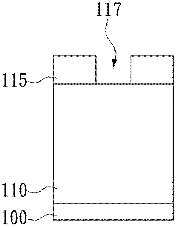
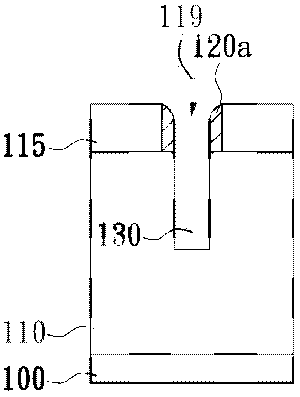
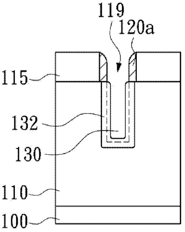
A method for manufacturing a trench power metal-oxide semiconductor field-effect transistor includes forming a pattern layer on a substrate; etching the substrate via the pattern layer to form a gate trench in the substrate; forming a first oxide layer in the gate trench in an oxidation manner to increase the width of the gate trench; forming a gate oxide layer on the inner surface of the gate trench after the first oxide layer is removed; etching the bottom of the gate trench via the pattern layer to form an opening penetrating through the gate oxide layer; then forming a thick oxide layer in the opening; and forming two first heavily doped regions on two sides of the thick oxide layer in an ion implantation mode to prevent a body region from being diffused to the bottom of the gate trench. The method has the advantages that the thickness of an insulating layer between a gate electrode and a drain electrode can be increased, accordingly, capacitance of the gate electrode to the drain electrode is reduced, and switching loss is decreased.

Description

technical field [0001] The invention relates to a method for manufacturing a trench-type power metal-oxygen-semiconductor field-effect transistor, in particular to a method for manufacturing a trench-type power metal-oxygen-semiconductor field-effect transistor that can reduce the switching loss of the metal-oxygen-semiconductor field-effect transistor. Background technique [0002] Power MOSFETs are widely used in switching elements of power devices, such as power supplies, rectifiers, or low-voltage motor controllers. Today's power MOS field effect transistors mostly adopt a vertical structure design to increase device density. It utilizes the backside of the chip as the drain, and manufactures the sources and gates of multiple transistor elements on the front side of the chip. Since the drains of each transistor element are connected in parallel, their withstand current can be increased. [0003] The operating loss of power MOSFETs can be divided into two categories: sw...

Claims


Application Information

Patent Timeline
Patent Type & Authority Patents(China)
IPC IPC(8): H01L21/336
Inventor 张渊舜蔡依芸涂高维许修文
Owner SUPER GROUP SEMICON
Why Eureka
Try Eureka