Array substrate and fabrication method thereof and display panel

A technology of an array substrate and a manufacturing method, which is applied in the field of display panels and can solve problems affecting product quality, etc.

Active Publication Date: 2014-10-15
BOE TECH GRP CO LTD +1
View PDF4 Cites 6 Cited by
  • Summary
  • Abstract
  • Description
  • Claims
  • Application Information

AI Technical Summary

Problems solved by technology

[0009] In the above-mentioned process of forming the pixel electrode 9, when the ITO film is etched, it is easy to produce etching residues 10 (such as Figure 5 As shown), the phenomenon of interconnection between the pixel electrodes 9 is generated, which affects the product quality

Method used


Image

  • Array substrate and fabrication method thereof and display panel
  • Array substrate and fabrication method thereof and display panel
  • Array substrate and fabrication method thereof and display panel

Examples


specific Embodiment approach

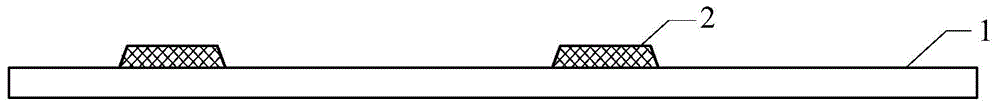
[0064] In the present invention, the strip electrodes may be pixel electrodes or common electrodes. As a specific embodiment of the present invention, the strip electrodes are pixel electrodes 9 .

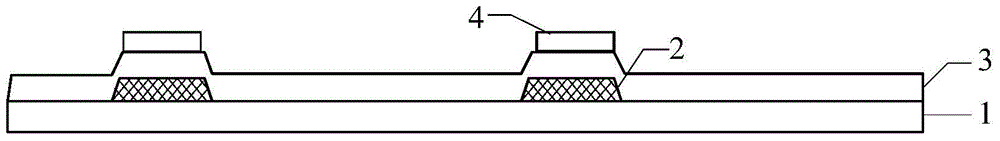
[0065] When the strip electrode is a pixel electrode 9, in order to connect the pixel electrode 9 to the drain electrode 5 of the thin film transistor, a via hole can be formed on the insulating layer 7 to expose a part of the drain electrode 6 so as to be connected to the pixel electrode 9. connected. The strip-shaped electrode area of ​​the insulating layer 7 may include a via sub-area for forming a via 8, and the step S32 may include:

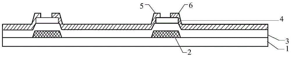
[0066] S321, exposing and developing the photoresist, so that the thickness of the photoresist in the interval region after development is greater than the thickness of the photoresist in the strip electrode region, and remove the photoresist in the via hole region (Such as Figure 7 shown);

[0067] S323, ashing the photoresist to remove the ...


PUM

PropertyMeasurementUnit
thicknessaaaaaaaaaa
thicknessaaaaaaaaaa

Abstract

The invention provides an array substrate and a fabrication method thereof and a display panel. The array substrate comprises a plurality of thin film transistors, and the fabrication method of the array substrate comprises the steps of: S1, providing the substrate, wherein sources and drains of the thin film transistors are formed on the substrate; S2, forming an insulation layer on the substrate, wherein the insulation layer comprises interval regions and a plurality of strip electrode regions, two arbitrary adjacent strip electrode regions are separated by the interval regions; S3, forming interval layers above the interval regions of the insulation layer; S4, forming patterns containing strip electrodes above the strip electrode regions of the insulation layer; and S5, stripping the interval layers above the interval regions. By the array substrate and the fabrication method thereof, the strip electrodes can be prevented from being connected to one another due to etching residue, and product feature is further improved.

Description

technical field [0001] The invention relates to the technical field of display manufacturing, in particular to a method for manufacturing an array substrate, an array substrate obtained by the method, and a display panel including the array substrate. Background technique [0002] At present, the array substrate of Thin Film Transistor Liquid Crystal Display (TFT-LCD) is completed through multiple patterning processes, wherein each patterning process includes: photoresist coating, exposure, development, engraving, etc. etching and stripping processes. [0003] Generally, the fabrication of the array substrate can be completed through four, five or six patterning processes. The method for forming the array substrate through five patterning processes includes: [0004] First, gate metal is deposited on the substrate 1, and the pattern of the gate 2 is formed through the first patterning process, such as figure 1 shown; [0005] Secondly, deposit an insulating material (SiN...

Claims


Application Information

Patent Timeline
Patent Type & Authority Applications(China)
IPC IPC(8): H01L21/77H01L27/12
CPCH01L27/1248H01L27/1259H01L27/124H01L27/127
Inventor 张鹏举赵雨高紫龙
Owner BOE TECH GRP CO LTD
Why Eureka
Try Eureka