Method of manufacturing solar cell

A technology for solar cells and manufacturing methods, applied in the direction of final product manufacturing, sustainable manufacturing/processing, circuits, etc., can solve problems such as affecting the reliability of solar modules, poor bonding force, and difficulty in the packaging process of solar cells

Inactive Publication Date: 2014-10-22
MOTECH INDUSTRIES
View PDF4 Cites 1 Cited by
  • Summary
  • Abstract
  • Description
  • Claims
  • Application Information

AI Technical Summary

Problems solved by technology

In this way, not only will it cause difficulties in the subsequent module encapsulation process of the solar cell, but also because the joint area between the conductive portion 104 and the conductive strip 110 is reduced, resulting in a gap between the conductive strip 110 and the conductive portion 104 of the solar cell. Poor bonding force, which in turn affects the reliability of the resulting solar module

Method used


Image

  • Method of manufacturing solar cell
  • Method of manufacturing solar cell
  • Method of manufacturing solar cell

Examples


Embodiment Construction

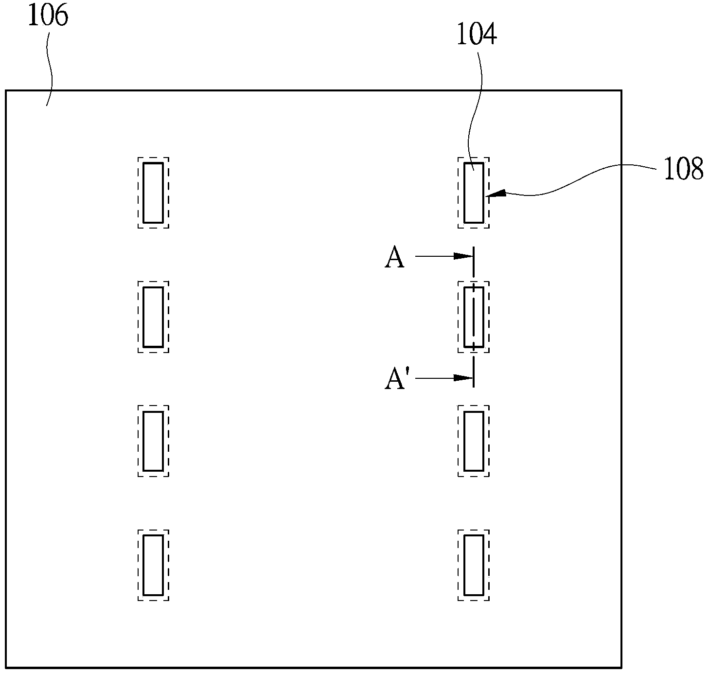
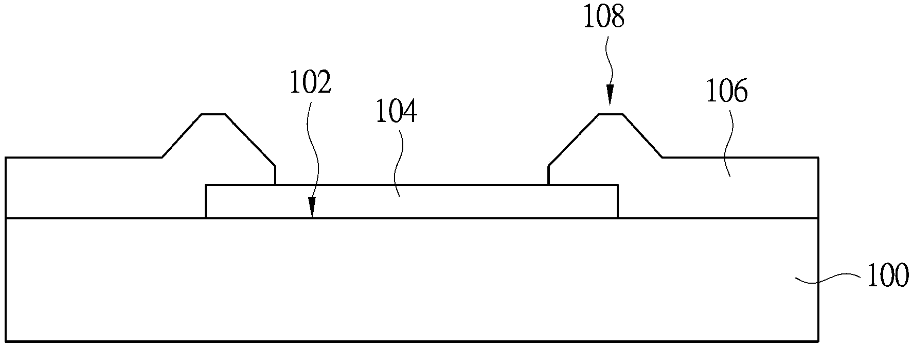
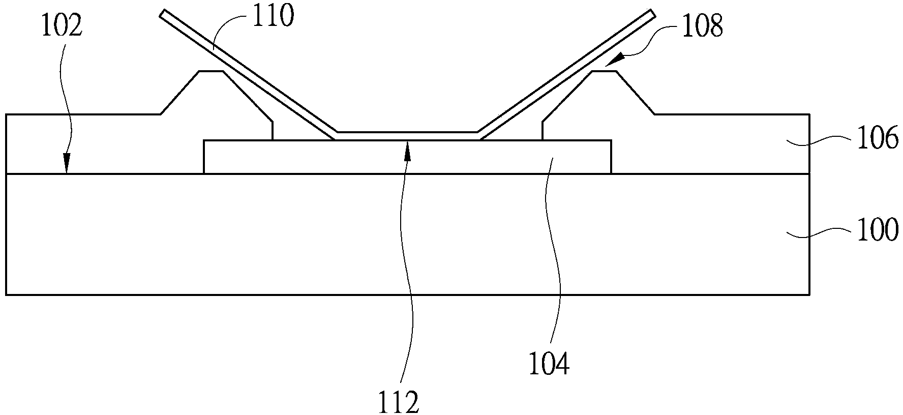
[0046] Please refer to Figure 3A to Figure 3C , which is a cross-sectional view illustrating a process of a solar cell according to an embodiment of the present invention. In this embodiment, when manufacturing a solar cell, the photoelectric conversion substrate 200 may be prepared first, wherein the photoelectric conversion substrate 200 has a P / N junction structure to convert light energy such as sunlight into electrical energy. Such as Figure 3A As shown, the photoelectric conversion substrate 200 includes a light-receiving surface 204 and a backlight surface 202 respectively located on two opposite sides of the photoelectric conversion substrate 200 . The light-receiving surface 204 of the photoelectric conversion substrate 200 is a surface receiving incident light from a light source such as sunlight, and the backlight surface 202 is a surface facing away from the incident light. In the photoelectric conversion substrate 200 , the light-receiving surface 204 is usual...


PUM


Abstract

A method of manufacturing solar cells comprises the steps of preparing a photovoltaic conversion substrate, and forming a collector layer and multiple conductive portions on a backlight surface of the photovoltaic conversion substrate, wherein the multiple conductive portions are arranged at intervals in a direction. The collector layer is formed by a screen plating process of a collector layer screen plating plate. The collector layer is equipped with multiple openings at intervals, includes multiple first collector portions that are correspondingly adjacent to the multiple openings respectively, and also includes a second collector portion which is thicker than each first collector portion. Each conductive portion overlaps at least one opening and at least one first collector portion. The collector layer screen plating plate is divided into multiple spaced non-sink-deposit zones used for forming the multiple openings, multiple half-sink-deposit zones used for forming the multiple first collector portions, and a sink-deposit zone used for forming the second collector portion.

Description

technical field [0001] The present invention relates to a method for manufacturing a battery, and in particular to a method for manufacturing a semiconductor solar cell. Background technique [0002] In the solar cell manufacturing process, the screen printing technology is currently used to make the back collector layer and the conductive part. Please also refer to Figure 1A and Figure 1B , which are the top view of the back side of a conventional solar cell, and the Figure 1A The profile obtained by the A-A' section line. In this technology, when fabricating the collector layer 106 and the conductive portion 104 on the back of the solar cell, the conductive portion 104 may be formed on the partial surface 102 of the substrate 100 by screen printing. Next, the collector layer 106 is also formed on a partial area of ​​the surface 102 of the substrate 100 by screen printing. Except for the collector layer 106 covering the surface 102 of the substrate 100 except for the ...

Claims


Application Information

Patent Timeline
Patent Type & Authority Applications(China)
IPC IPC(8): H01L31/18
CPCH01L31/02008H01L31/022425Y02E10/50Y02P70/50
Inventor 柳彦志曹铭修赖政豪张冠纶江一志王宗昶黄宏钦黄馨慧叶耿伟
Owner MOTECH INDUSTRIES
Why Eureka
Try Eureka