MOS transistor and forming method thereof

A MOS transistor and semiconductor technology, which is applied in the direction of semiconductor devices, semiconductor/solid-state device manufacturing, electrical components, etc., can solve the problems of drain induction barrier reduction, affecting transistor performance and reliability, source-drain punch-through, etc., to avoid source Drain punch-through effect, the effect of improving the short channel effect

Inactive Publication Date: 2014-10-29
SEMICON MFG INT (SHANGHAI) CORP
View PDF4 Cites 23 Cited by
  • Summary
  • Abstract
  • Description
  • Claims
  • Application Information

AI Technical Summary

Problems solved by technology

[0008] The MOS transistor formed by the existing technology is prone to lowering of the drain induction barri

Method used


Image

  • MOS transistor and forming method thereof
  • MOS transistor and forming method thereof
  • MOS transistor and forming method thereof

Examples


Example Embodiment

[0035] As mentioned in the background art, phenomena such as source-drain punch-through and drain-induced barrier reduction of MOS transistors formed in the prior art will seriously affect the performance and reliability of the transistor.
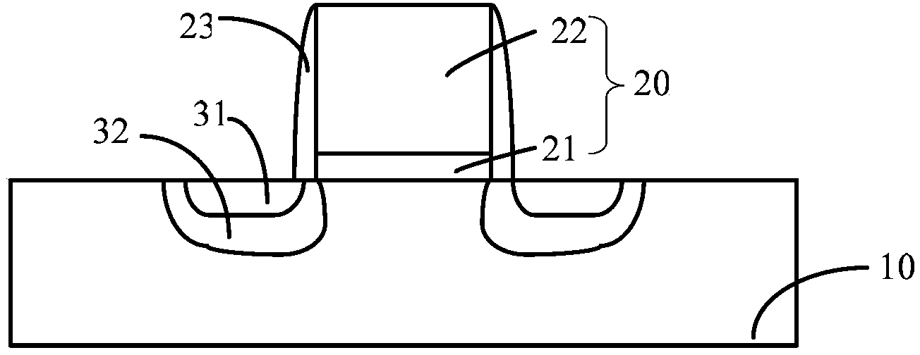
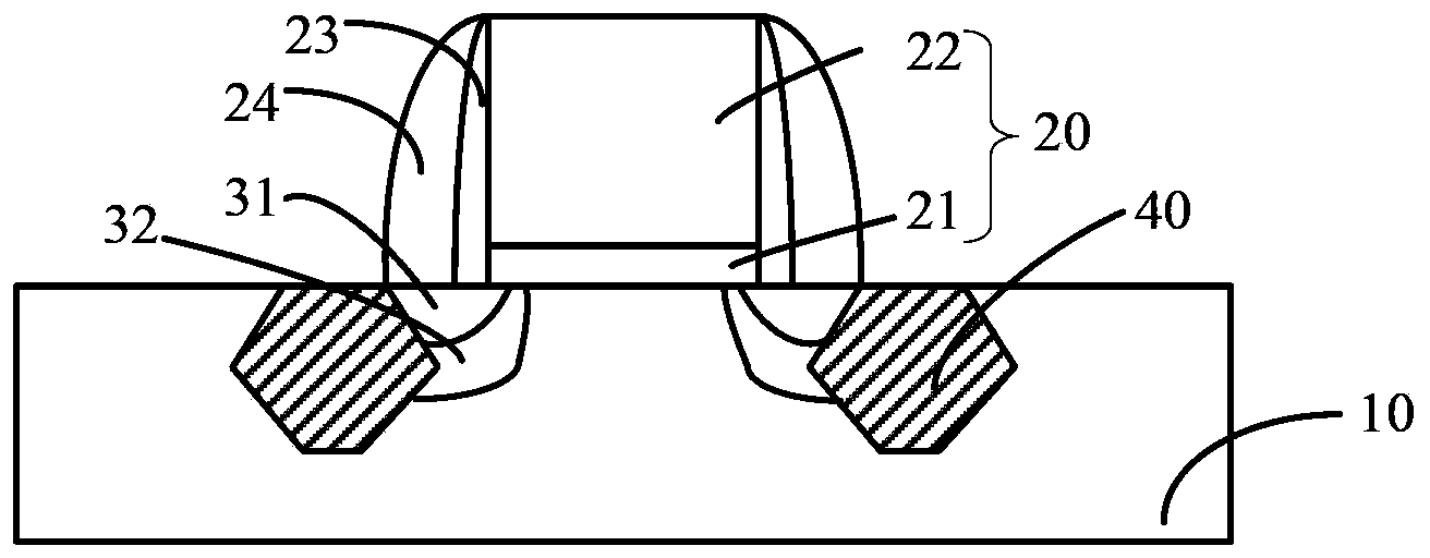
[0036] Studies have found that in the prior art, after forming the lightly doped region and the halo region of the transistor, the source and drain of the transistor are formed by the SiGe or SiC source-drain process, and the short channel effect of the transistor is serious. Mainly because in the process of forming the source and drain of the transistor, the semiconductor substrate needs to be etched to form a groove. When the semiconductor substrate is etched to form the groove, it is inevitable to remove some of the halo formed before. The area of ​​the halo region is reduced, and the diffusion barrier to the source and drain doped ions is also reduced accordingly; and since the depth of the source and drain formed is greater than the depth...


PUM

PropertyMeasurementUnit
Thicknessaaaaaaaaaa

Abstract

Provided are an MOS transistor and a forming method thereof. The method for forming the MOS transistor comprises the steps of providing a semiconductor substrate and enabling the surface of the semiconductor substrate to be provided with a grid structure; etching the semiconductor substrate on two sides of the grid structure to form grooves; forming a diffusion barrier layer on the surface of a side wall of one side of each groove close to the grid structure, enabling the diffusion barrier layer to cover two sides of a channel area; and forming sources and drains in the grooves. The method for forming the MOS transistor can improve short channel effect of the transistor and improve performance of the transistor.

Description

technical field [0001] The invention relates to the technical field of semiconductors, in particular to a MOS transistor and a forming method thereof. Background technique [0002] With the continuous development of semiconductor technology, the degree of integration of integrated circuits is getting higher and higher, and the size of devices is also decreasing. However, the continuous reduction of device size has greatly affected the performance of the device. For example, when the length of the channel shrinks to a certain extent, the device begins to show short-channel effects, including the decrease of carrier mobility, the increase of threshold voltage, and the decrease of drain-induced barrier (DIBL). [0003] In the existing MOS manufacturing process, in order to suppress the short channel effect, lightly doped source / drain (LDD) and halo (Halo) implants are usually used to form a lightly doped region before the source / drain of the transistor is formed. and the halo...

Claims


Application Information

Patent Timeline
IPC IPC(8): H01L21/336H01L21/265H01L29/78
CPCH01L29/66636H01L29/0642H01L29/7816
Inventor 赵猛
Owner SEMICON MFG INT (SHANGHAI) CORP
Why Eureka
Try Eureka