Organic light emitting diode display and method of manufacturing the same

A technology of light-emitting diodes and displays, which is applied in semiconductor/solid-state device manufacturing, electric solid-state devices, semiconductor devices, etc., and can solve problems such as residues

Inactive Publication Date: 2014-10-29
SAMSUNG DISPLAY CO LTD
View PDF3 Cites 6 Cited by
  • Summary
  • Abstract
  • Description
  • Claims
  • Application Information

AI Technical Summary

Problems solved by technology

[0007] However, the portion of the organic layer that needs to be transferred to the display substrate using a laser may remain in the transfer layer during the transfer process.

Method used


Image

  • Organic light emitting diode display and method of manufacturing the same
  • Organic light emitting diode display and method of manufacturing the same
  • Organic light emitting diode display and method of manufacturing the same

Examples


Embodiment Construction

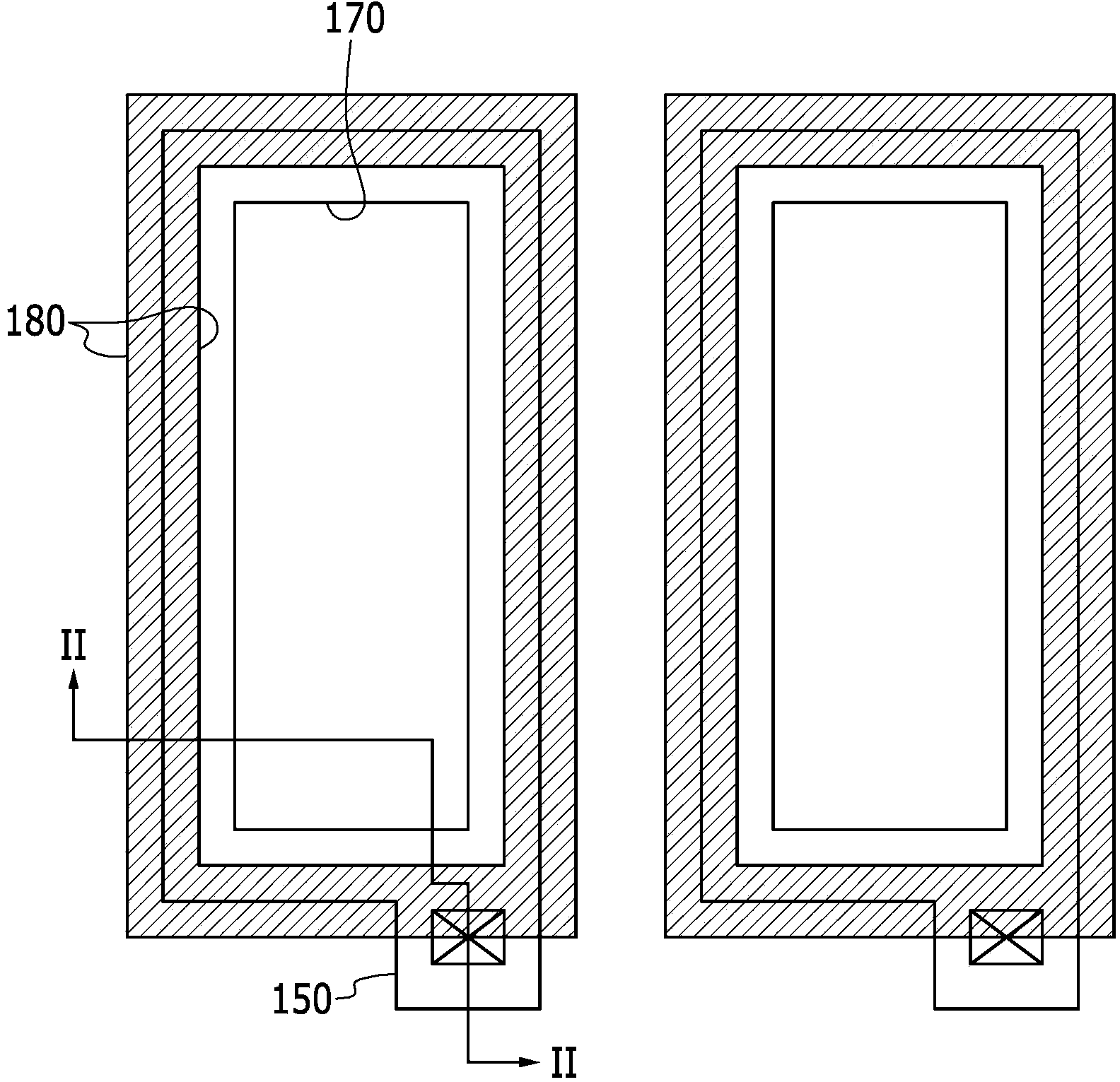
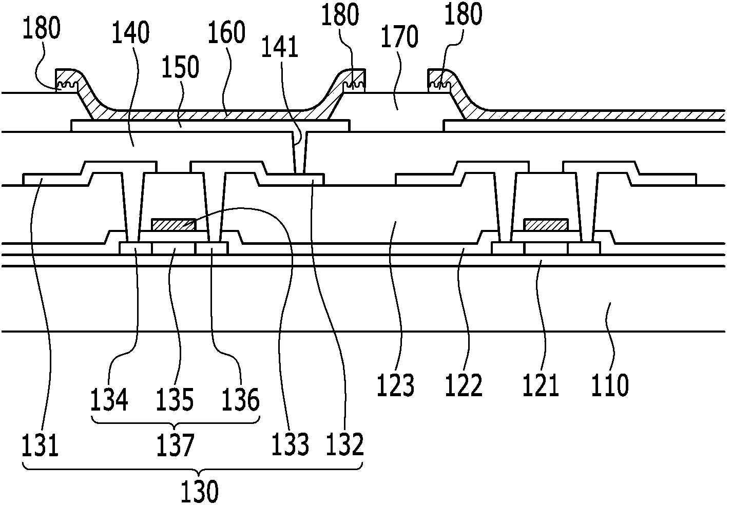
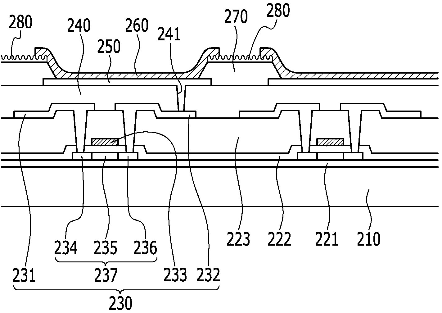
[0035] The present invention will be described more fully hereinafter with reference to the accompanying drawings, in which exemplary embodiments of the present invention are shown. As those skilled in the art will realize, the described embodiments may be modified in various different ways without departing from the spirit or scope of the present invention. The drawings and description should be regarded as illustrative in nature and not restrictive. Throughout the specification, the same reference numerals designate the same elements.

[0036] In the drawings, the size and thickness of components are exaggerated, omitted or schematically shown for clarity and convenience of description. In addition, the size of the constituent elements does not completely reflect its actual size.

[0037] In the drawings, the thickness of layers, films, panels, regions, etc., are exaggerated for clarity. In addition, in order to make the description easier and better understood, the thickness ...


PUM


Abstract

An organic light-emitting diode (OLED) display according to an exemplary embodiment of the present invention includes a substrate, a thin film transistor formed on the substrate, a pixel electrode formed on the thin film transistor and electrically connected to the thin film transistor, a pixel definition layer formed on the pixel electrode so as to define a pixel region, an emission layer formed on the pixel electrode and contacting the pixel electrode in the pixel region, and an interlayer formed on the pixel definition layer and contacting part of the emission layer. One side of the interlayer has an uneven shape so that a surface area of the interlayer is increased.

Description

Technical field [0001] The invention relates to an organic light emitting diode (OLED) display and a manufacturing method thereof. Background technique [0002] The OLED used in flat panel displays includes an anode, a cathode, and an organic layer interposed between the anode and the cathode. In addition to the emission layer, the organic layer also includes a hole injection layer (HIL), a hole transport layer (HTL), an electron transport layer (ETL), and an electron injection layer (EIL). According to the composition of the organic layer (specifically, the emission layer), OLEDs are classified into polymer OLEDs and low molecular weight OLEDs. [0003] In order to achieve full color, the organic layer needs to be patterned on the substrate. A shadow mask is used to pattern the organic layer of the low molecular weight OLED. Use inkjet printing or laser induced thermal imaging (LITI) to pattern the organic layer of the polymer OLED. [0004] Unlike the wet process of inkjet prin...

Claims


Application Information

Patent Timeline
Patent Type & Authority Applications(China)
IPC IPC(8): H01L27/32H01L51/52H01L51/56
CPCH01L27/3262H10K59/122H10K59/353H10K59/127H10K59/10H10K71/18H10K30/865H10K50/13H10K50/11H10K71/851H10K71/00
Inventor 金南珍朴彻桓
Owner SAMSUNG DISPLAY CO LTD
Why Eureka
Try Eureka