Pixel structure, array substrate and display device

A pixel structure and array substrate technology, which is applied in the field of array substrates, display devices, and pixel structures, can solve the problems of increasing the aperture ratio, and achieve the effects of improving the display effect, reducing light leakage, and increasing the aperture ratio

Inactive Publication Date: 2014-11-05
TRULY SEMICON
View PDF6 Cites 9 Cited by
  • Summary
  • Abstract
  • Description
  • Claims
  • Application Information

AI Technical Summary

Problems solved by technology

The aperture ratio of the existing pixel structure needs to be increased

Method used


Image

  • Pixel structure, array substrate and display device
  • Pixel structure, array substrate and display device
  • Pixel structure, array substrate and display device

Examples


Embodiment Construction

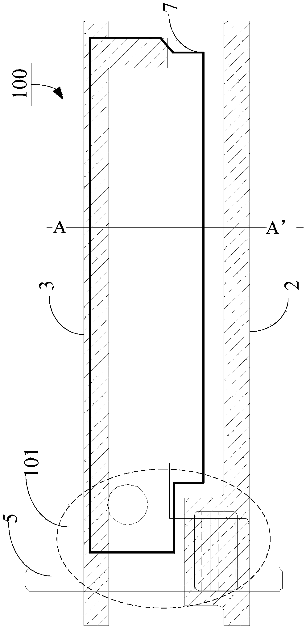
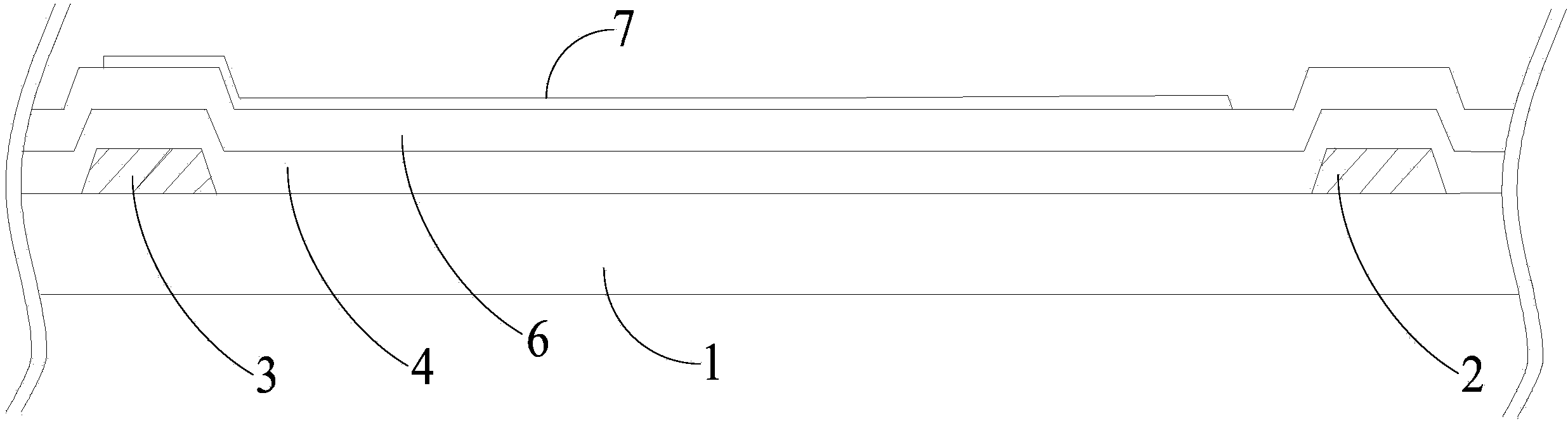
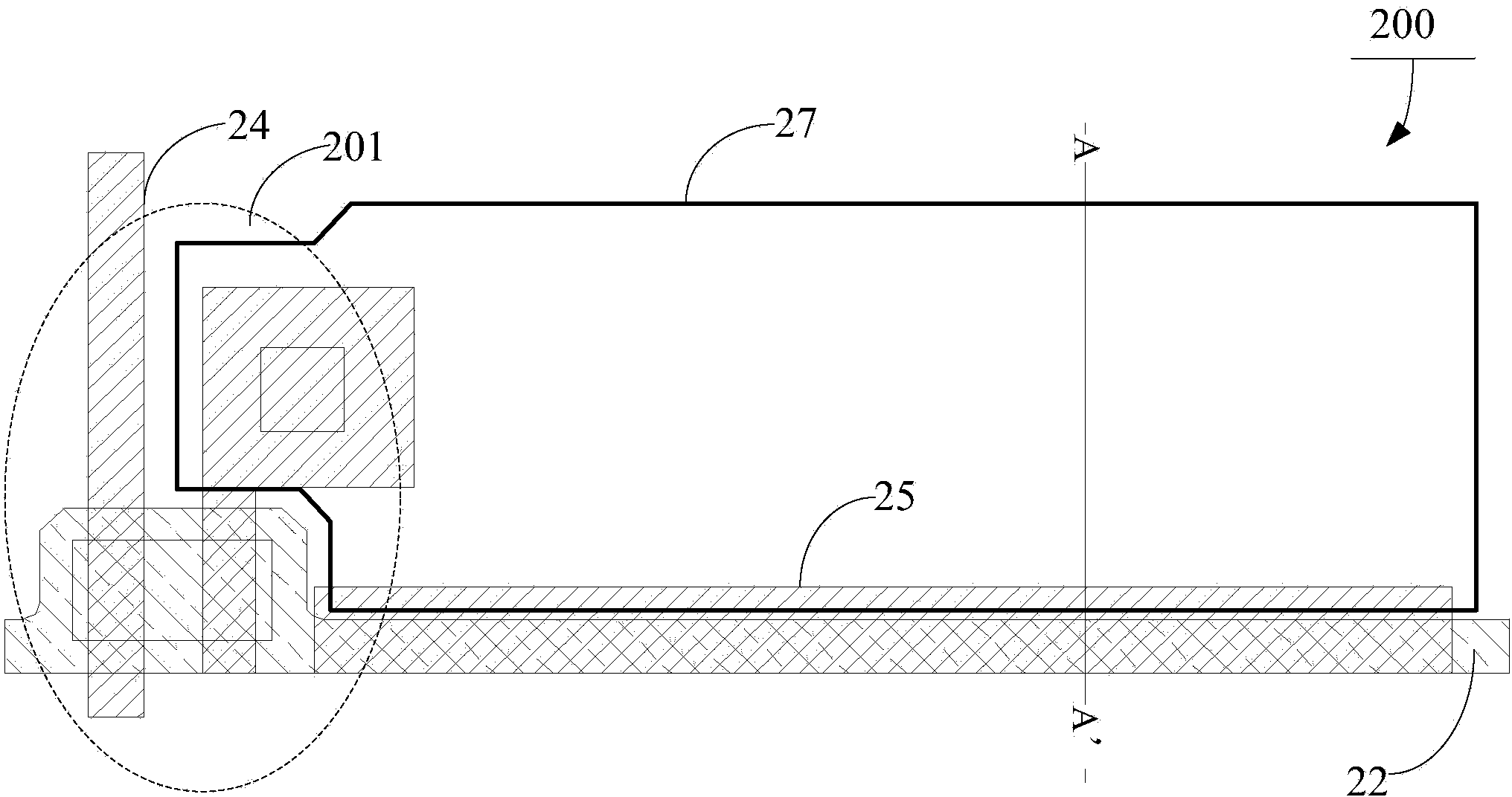
[0030] As mentioned in the background art, the aperture ratio of the existing laterally arranged pixel structure needs to be increased. The inventors found that the cause of this defect is mainly due to the fact that in the existing pixel structure, the common electrode and the gate line are located in the same conductive layer, and the common electrode and the gate line are isolated from each other, so the same distance between the gate line and the common electrode The plane situation increases the light-shielding area and reduces the light-transmitting area, thereby reducing the aperture ratio of the pixel structure.

[0031] Based on this, the present invention provides a pixel structure to overcome the above-mentioned problems in the prior art. The pixel structure includes:

[0032] Gate lines, data lines, pixel electrodes and common electrodes;

[0033] The common electrode is formed between the conductive layer where the gate line is located and the conductive layer wh...


PUM


Abstract

The invention discloses a pixel structure, an array substrate and a display device. The pixel structure comprises a gate line, a data line, a pixel electrode and a common electrode. The common electrode is formed between a conducting layer where the gate line is placed and a conducting layer where the pixel electrode is placed, the common electrode is both isolated from the gate line and the pixel electrode, the gate line is covered with the common electrode, and the common electrode and the pixel electrode form an overlapping area. Due to the fact that the common electrode is formed above the gate line, compared with the condition that an existing common electrode and a gate line are placed on the same conducting layer, the aperture ratio of the pixel structure can be increased, the common electrode can further play a certain shading effect, light leakage at the edge area of the pixel structure is reduced, the contrast ratio, the transmittance and the display stability of the display device are improved, and the display effect of the display device is improved.

Description

technical field [0001] The present invention relates to the field of display technology, and more specifically, to a pixel structure, an array substrate and a display device. Background technique [0002] Liquid crystal display has the characteristics of light and thin, low radiation, low power consumption, etc., and has replaced the traditional cathode ray tube display to become the mainstream product in the display market. As one of the components of the liquid crystal display device, the array substrate is of great significance. [0003] combine Figure 1a with 1b as shown, Figure 1a is a structural schematic diagram of an existing pixel structure; Figure 1b for Figure 1a Sectional view of the provided pixel structure along the direction AA'. Wherein, the pixel structure is a horizontal pixel structure, and the array substrate includes a plurality of pixel structures 100 , and the pixel structures 100 include thin film field effect transistors 101 . [0004] Wherei...

Claims


Application Information

Patent Timeline
Patent Type & Authority Applications(China)
IPC IPC(8): G02F1/1362G02F1/1343H01L27/12
CPCG02F1/1343G02F1/1362H01L27/12
Inventor 庄崇营胡君文李林洪胜宝何基强李建华
Owner TRULY SEMICON
Why Eureka
Try Eureka