AMOLED (Active Matrix Organic Light Emitting Diode) pixel structure and manufacturing method thereof
A pixel structure and pixel technology, applied in the direction of instruments, electrical components, electric solid devices, etc., can solve the problems of limitation and low aperture ratio, and achieve the effect of optimizing position, improving aperture ratio, and reducing area
- Summary
- Abstract
- Description
- Claims
- Application Information
AI Technical Summary
Problems solved by technology
Method used
Image
Examples
Embodiment Construction
[0022] The embodiments of the present invention are designed according to the principles of the present invention, and the present invention will be further described below in conjunction with the drawings and specific embodiments.
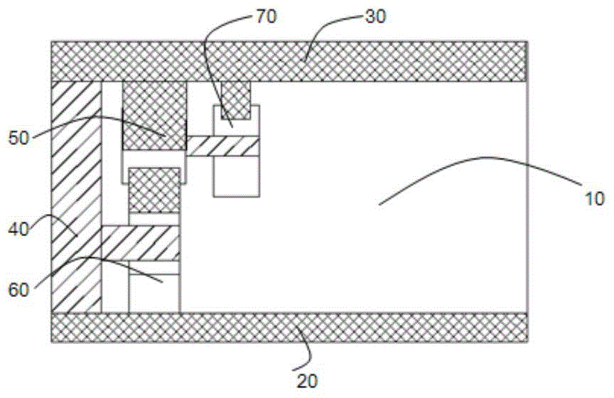
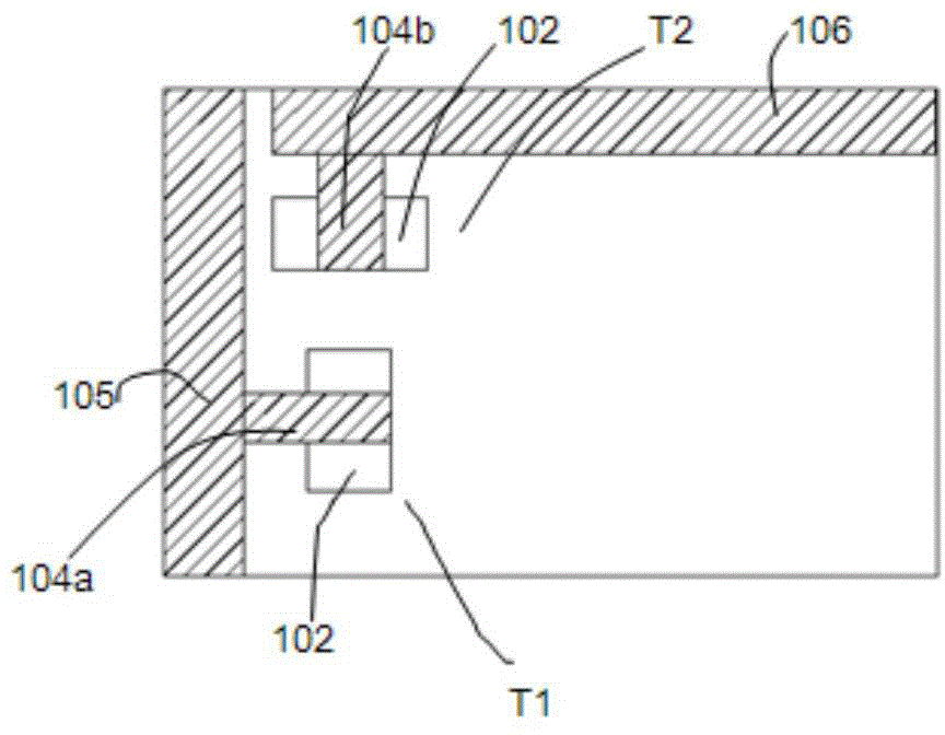
[0023] An AMOLED pixel structure in this embodiment includes a pixel light-emitting area, a power supply line VDD, a scanning line SCAN, a data line DATA, a switching transistor, a driving transistor, and a storage capacitor. The metal of the power supply line VDD forms the upper electrode of the storage capacitor and is located at A corresponding metal layer is included directly under the metal of the power line VDD as the lower electrode of the storage capacitor, and an interval dielectric ILD is included between the upper electrode and the lower electrode. In order to make the pixel area compact and optimize the pixel display structure, the switch transistor and drive transistor are transferred to the location of the storage capacitor in the 2T1...
PUM
 Abstract
Description
Claims
Application Information


