A light-emitting diode epitaxial wafer and its manufacturing method

A technology of light emitting diodes and epitaxial wafers, applied in electrical components, circuits, semiconductor devices, etc., can solve the problems of low luminous efficiency of LEDs, and achieve the effects of improving luminous efficiency, improving secondary light emitting efficiency, and increasing the probability of

Active Publication Date: 2017-04-26
HC SEMITEK CORP
View PDF3 Cites 0 Cited by
  • Summary
  • Abstract
  • Description
  • Claims
  • Application Information

AI Technical Summary

Problems solved by technology

[0006] In order to solve the problem of low luminous efficiency of LEDs in the prior art, an embodiment of the present invention provides a light-emitting diode epitaxial wafer and a manufacturing method thereof

Method used


Image

  • A light-emitting diode epitaxial wafer and its manufacturing method
  • A light-emitting diode epitaxial wafer and its manufacturing method

Examples


Embodiment 1

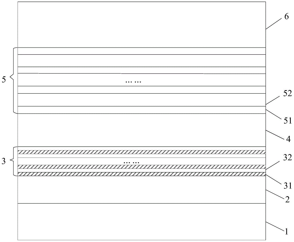
[0025] An embodiment of the present invention provides an LED epitaxial wafer, see figure 1 , the epitaxial wafer includes a sapphire substrate 1, and an undoped GaN layer 2, a superlattice GaN layer 3, an N-type GaN layer 4, an active layer 5, and a P-type GaN layer 6 sequentially stacked on the sapphire substrate 1 .

[0026] In this embodiment, the growth temperature of the superlattice GaN layer 3 is 750-1050° C., and the superlattice GaN layer 3 includes alternately grown first GaN layers 31 (indicated by hatching) and second GaN layers 32, the first The GaN layer 31 is grown in a 3D (three-dimensional) mode, and the second GaN layer 32 is grown in a 2D (two-dimensional) mode. The active layer 5 is an alternately grown InGaN layer 51 and a GaN layer 52 .

[0027] Specifically, the Ga content of the first GaN layer 31 may be 1 / 3-1 / 2 of the Ga content of the second GaN layer 32 .

[0028] Optionally, the total number of layers of the first GaN layer 31 and the second GaN...

Embodiment 2

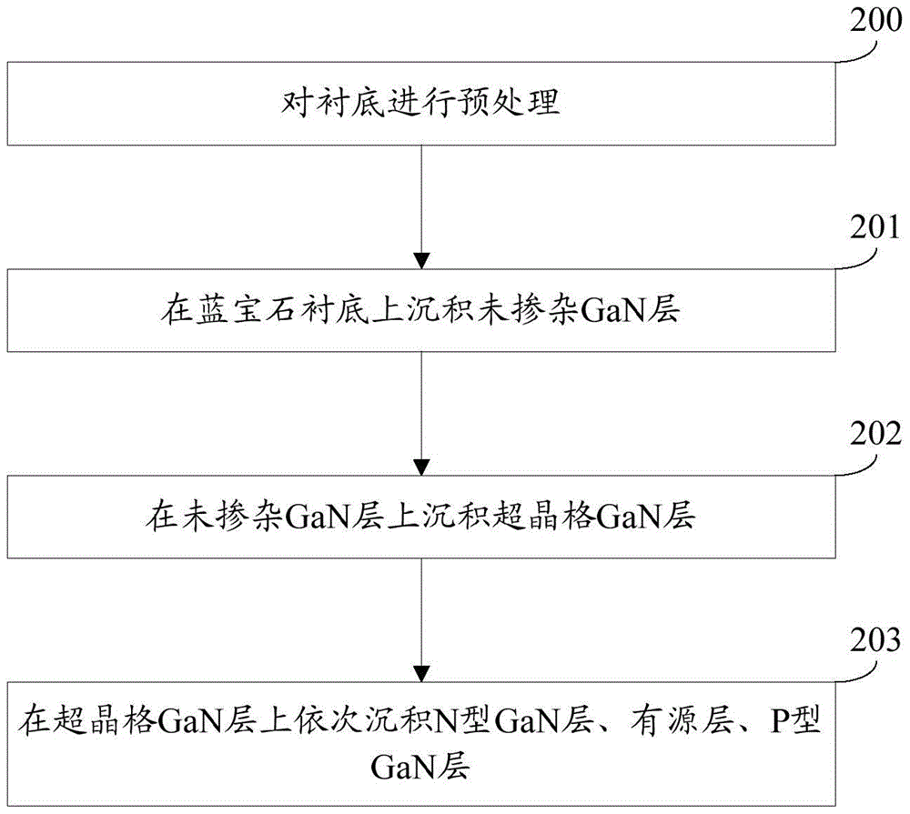
[0034] An embodiment of the present invention provides a method for manufacturing an LED epitaxial wafer, which is suitable for manufacturing the LED epitaxial wafer provided in Embodiment 1, see figure 2 , the method includes:

[0035] Step 200: pretreating the sapphire substrate.

[0036] Specifically, this step 200 may include:

[0037] Put the sapphire substrate into a MOCVD (Metal Organic Chemical Vapor Deposition, metal organic compound chemical vapor deposition) system, and heat-treat at high temperature for 10-15 minutes.

[0038] For example, in an MOCVD system, a sapphire substrate is treated at a temperature of 1100°C in a pure hydrogen atmosphere for 15 minutes.

[0039] Step 201: Deposit an undoped GaN layer on a sapphire substrate.

[0040] Specifically, this step 201 may include:

[0041] 3 μm GaN was grown at 1000°C.

[0042] Optionally, before step 201, the method may also include:

[0043] 20nm GaN was grown at 600°C.

[0044] Step 202: Deposit a supe...


PUM


Abstract

The invention discloses a light-emitting diode epitaxial wafer and a manufacturing method thereof, belonging to the technical field of semiconductors. The epitaxial wafer includes a sapphire substrate, and an undoped GaN layer, an N-type GaN layer, an active layer, and a P-type GaN layer sequentially stacked on the sapphire substrate, and the active layer is an alternately grown InGaN layer and a GaN layer , the epitaxial wafer also includes a superlattice GaN layer, the superlattice GaN layer is laminated between the undoped GaN layer and the N-type GaN layer, and the superlattice GaN layer includes alternately grown first GaN layers and second GaN layers, The first GaN layer is grown in a three-dimensional 3D mode, and the second GaN layer is grown in a two-dimensional 2D mode. By inserting a GaN layer grown in a 3D mode, the present invention can deflect and merge dislocations on the one hand, and on the other hand, effectively change the direction of light reflected back by total reflection, so as to re-emit, thereby improving the luminous efficiency of the LED.

Description

technical field [0001] The invention relates to the technical field of semiconductors, in particular to a light-emitting diode epitaxial wafer and a manufacturing method thereof. Background technique [0002] LED (Light Emitting Diode, Light Emitting Diode) is a semiconductor electronic component that can emit light. It has the characteristics of small size, high brightness and low energy consumption. It is widely used in the fields of display screens, backlight sources and lighting. [0003] The existing LED epitaxial wafer includes a sapphire substrate, and an undoped GaN layer, an N-type GaN layer, an active layer, and a P-type GaN layer grown on the substrate in sequence. Wherein, the active layer is an alternately grown InGaN layer and a GaN layer. [0004] In the process of realizing the present invention, the inventor finds that there are at least the following problems in the prior art: [0005] The substrate material sapphire and other layer materials GaN are hete...

Claims


Application Information

Patent Timeline
Patent Type & Authority Patents(China)
IPC IPC(8): H01L33/04H01L33/10H01L33/00
CPCH01L33/007H01L33/06H01L33/10
Inventor 吴克敏谢文明陈柏松魏世祯
Owner HC SEMITEK CORP
Why Eureka
Try Eureka