Epitaxial wafer, epitaxial wafer preparation method and blue-green light emitting diode

A technology of epitaxial wafers and sub-layers, applied in chemical instruments and methods, post-processing details, crystal growth, etc., can solve the problems of low electron-hole radiation recombination efficiency, reduce electron overflow, improve interface quality, and improve electron density. Effect of hole radiative recombination efficiency

Pending Publication Date: 2022-07-22
JIANGXI ZHAO CHI SEMICON CO LTD
View PDF0 Cites 0 Cited by
  • Summary
  • Abstract
  • Description
  • Claims
  • Application Information

AI Technical Summary

Problems solved by technology

[0005] In view of this, the object of the present invention is to provide an epitaxial wafer, a preparation method of the epitaxial wafer and a blue-green light-emitting diode, aiming at solving the problem of low electron-hole radiation recombination efficiency of the epitaxial wafer in the prior art

Method used


Image

  • Epitaxial wafer, epitaxial wafer preparation method and blue-green light emitting diode
  • Epitaxial wafer, epitaxial wafer preparation method and blue-green light emitting diode
  • Epitaxial wafer, epitaxial wafer preparation method and blue-green light emitting diode

Examples


Embodiment 1

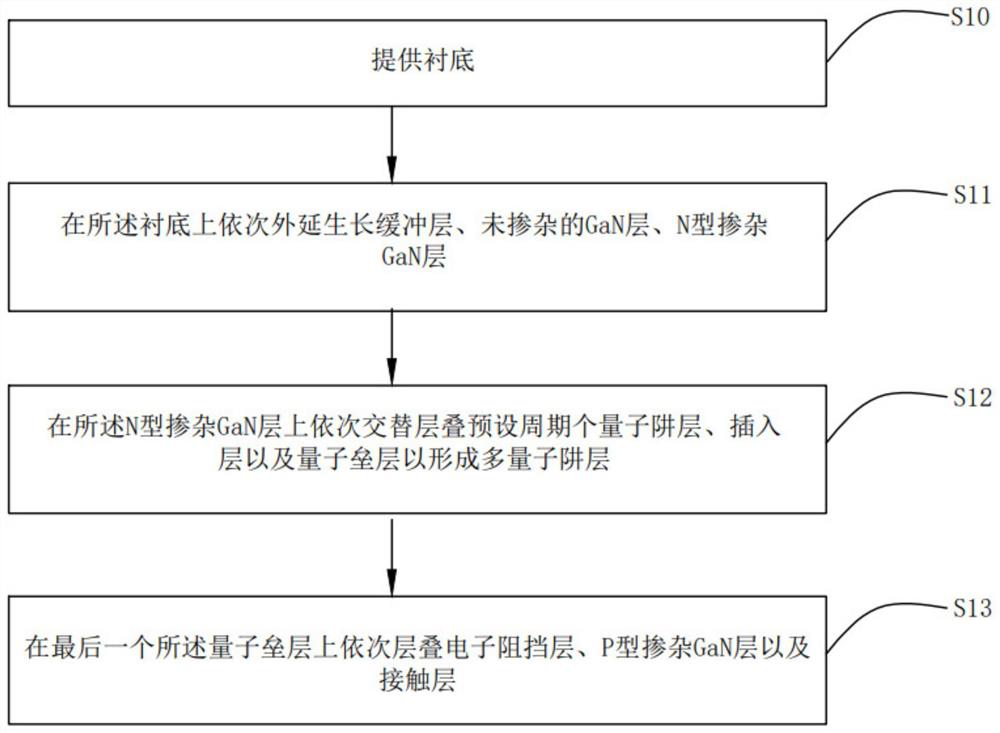
[0065] provide a substrate;

[0066] The AlN layer is grown on the substrate by PVD to form the buffer layer, and then placed in the MOCVD system, and the undoped GaN layer, the N-type AlGaN layer, and the quantum well layer and the insertion layer are sequentially grown epitaxially on the buffer layer. and the quantum barrier layer, after the last quantum barrier layer is grown, the electron blocking layer, the P-type doped layer and the contact layer are grown in sequence.

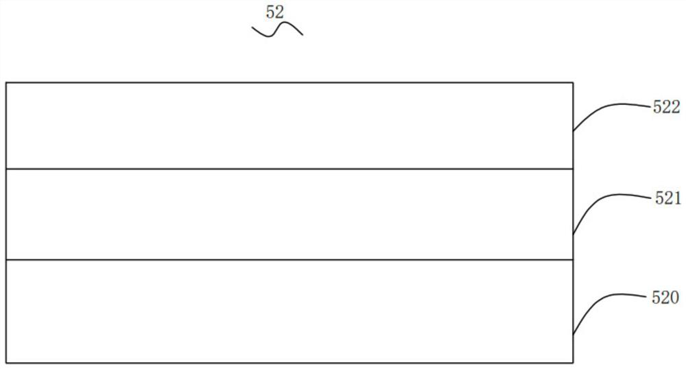
[0067] Wherein, when growing the insertion layer, an AlN layer with a thickness of 1 nm is first grown under the conditions of a growth temperature of 900° C. and a growth pressure of 100 torr to form a first insertion sub-layer, and then a growth temperature of 900° C. and a growth pressure of 100 torr A SiN layer with a thickness of 1 nm is grown to form a second insertion sub-layer under the conditions of Three insertion sublayers.

[0068] Among them, trimethylaluminum (TMAl), trimethylgallium or t...

Embodiment 2

[0070] The difference between the light-emitting diode epitaxial wafer and its preparation method in this embodiment and the light-emitting diode epitaxial wafer and its preparation method in Example 1 is:

[0071] The growth thickness of the first insertion sublayer is 0.5 nm, the growth thickness of the second insertion sublayer is 1.0 nm, and the growth thickness of the third insertion sublayer is 2.0 nm.

Embodiment 3

[0073] The difference between the light-emitting diode epitaxial wafer and its preparation method in this embodiment and the light-emitting diode epitaxial wafer and its preparation method in Example 1 is:

[0074] The growth thickness of the first insertion sublayer is 0.5 nm, the growth thickness of the second insertion sublayer is 1.0 nm, and the growth thickness of the third insertion sublayer is 2.0 nm; The growth pressure of the inserted sublayers is all 50torr.


PUM

PropertyMeasurementUnit
thicknessaaaaaaaaaa
thicknessaaaaaaaaaa
thicknessaaaaaaaaaa

Abstract

The invention discloses an epitaxial wafer, an epitaxial wafer preparation method and a blue-green light emitting diode, the epitaxial wafer comprises a multi-quantum well layer, and the multi-quantum well layer comprises a quantum well layer, an insertion layer and a quantum barrier layer which are periodically, sequentially and alternately stacked; wherein the insertion layer comprises a first insertion sub-layer, a second insertion sub-layer and a third insertion sub-layer which are sequentially stacked on the quantum well layer, the quantum well layer is an InGaN layer, the quantum barrier layer is a GaN layer, the first insertion sub-layer and the third insertion sub-layer are both AlN layers, and the second insertion sub-layer is a SiN layer. According to the invention, the problem of low electron hole radiation recombination efficiency of the epitaxial wafer in the prior art is solved.

Description

technical field [0001] The invention relates to the technical field of semiconductors, in particular to an epitaxial wafer, a method for preparing the epitaxial wafer and a blue-green light emitting diode. Background technique [0002] GaN materials have been widely used in high-frequency, high-temperature, high-voltage electronic devices, light-emitting diodes (LEDs) due to their low heat generation efficiency, radiation resistance, high breakdown voltage, high electron saturation drift speed, and low dielectric constant. and semiconductor lasers (LD), etc., and have become the focus of current research. [0003] At present, there are many technical difficulties in the process of LED epitaxial growth, such as the existence of polarization electric field due to lattice mismatch between well barriers, which makes the energy band of the well barriers tilt, and the electron-hole distribution in the quantum wells is not uniform, resulting in The decrease in radiation recombinat...

Claims


Application Information

Patent Timeline
Patent Type & Authority Applications(China)
IPC IPC(8): H01L33/06C30B25/18C30B29/40C30B33/02H01L33/00H01L33/14
CPCH01L33/06H01L33/145H01L33/007H01L33/0095C30B29/406C30B25/186C30B33/02C30B29/403
Inventor 刘春杨胡加辉吕蒙普金从龙
Owner JIANGXI ZHAO CHI SEMICON CO LTD
Why Eureka
Try Eureka