A light emitting diode with a nitrogen polar face n-type electron blocking layer

A technology of electron blocking layer and light-emitting diode, which is applied in the direction of circuits, electrical components, semiconductor devices, etc., can solve the problems of radiation recombination efficiency and luminous efficiency reduction, reduction of carrier radiation recombination efficiency, heterojunction interface energy band bending, etc. , to achieve the effect of reducing the two-dimensional electron gas density, increasing the probability of radiative recombination, and increasing the effective potential barrier

Active Publication Date: 2022-07-01
SOUTHEAST UNIV
View PDF4 Cites 0 Cited by
  • Summary
  • Abstract
  • Description
  • Claims
  • Application Information

AI Technical Summary

Problems solved by technology

However, these electron blocking layers still cannot satisfactorily solve the following technical problems: 1) The traditional p-type electron blocking layer also reduces the hole injection efficiency while blocking electron leakage, resulting in the radiative recombination efficiency of carriers in the LED 2) The lattice mismatch between the multi-quantum well active region and the electron blocking layer is generally large, resulting in a strong polarization electric field in the active region, causing the energy band bending at the heterojunction interface, and electrons The wave function of the hole is separated in space, reducing the radiative recombination efficiency of the carrier, which is the so-called quantum-confined Stark effect; 3) In order to improve the hole injection efficiency, p-type electrons on the nitrogen polar surface are used The barrier layer often needs to be heavily doped with Mg to induce polarity reversal, which will cause Mg doping aggregation in the film, resulting in the deterioration of crystal quality

Method used


Image

  • A light emitting diode with a nitrogen polar face n-type electron blocking layer
  • A light emitting diode with a nitrogen polar face n-type electron blocking layer

Examples


Embodiment Construction

[0021] The present invention will be further explained below in conjunction with the accompanying drawings.

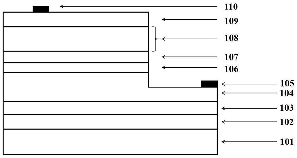
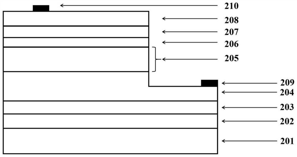
[0022] like figure 1 As shown, a light emitting diode with an n-type electron blocking layer on a nitrogen polar surface includes a substrate 101, a nitrogen polar surface nitride layer 102, a polarity inversion nitride layer 103, and a type nitride ohmic contact layer 104, n-type nitrogen polar surface electron blocking layer 106, undoped superlattice structure nitride layer 107, multiple quantum well active layer 108, p-type nitride ohmic contact layer 109, and n-type nitride ohmic contact layer 109 The n-type electrode 105 provided on the ohmic contact layer 104 of the nitride type and the p-type electrode 110 provided on the ohmic contact layer 109 of the p-type nitride.

[0023] The nitrogen polar surface nitride layer 102 is made of gallium nitride or aluminum nitride material with uniform composition. The thickness of the polarity-reversed nitride layer 103 i...


PUM

PropertyMeasurementUnit
thicknessaaaaaaaaaa
thicknessaaaaaaaaaa
thicknessaaaaaaaaaa

Abstract

The invention discloses a light emitting diode with a nitrogen polar surface n-type electron blocking layer, which comprises a substrate, a nitrogen polar nitride layer, a polarity inversion nitride layer, and an n-type nitride ohmic contact layer in order from bottom to top , n-type nitrogen polar surface electron blocking layer, non-doped superlattice structure layer, multiple quantum well active layer, p-type nitride ohmic contact layer. An n-type electrode and a p-type electrode are respectively provided on the n-type nitride ohmic contact layer and the p-type nitride ohmic contact layer. The n-type electron blocking layer with nitrogen polar face provided by the present invention can spatially limit the number of electrons entering the active region, and because the traditional p-type doped electron blocking layer is removed, it can increase the amount of electrons entering the active region. The injection rate of holes keeps the number of holes and electrons injected into the active region at a balanced level, which can improve the probability of electrons and holes in the active region radiating recombination light, thereby improving the performance of the light-emitting diode.

Description

technical field [0001] The invention provides a light emitting diode (LED) with a nitrogen polar plane n-type electron blocking layer, which belongs to the technical field of semiconductor optoelectronic materials and device manufacturing. Background technique [0002] Because LED has the advantages of high efficiency, energy saving, high reliability and long life, and has great advantages over traditional lighting sources in terms of energy saving, emission reduction and environmental protection, it has gradually replaced traditional lighting methods such as fluorescent lamps and incandescent lamps. . However, research shows that if figure 2 As shown, under the condition of high current injection, the internal quantum efficiency of LED decreases rapidly, and electrons can easily overcome the limitation of quantum wells to reach the p region for non-radiative recombination with holes. The main factors seriously restrict the application and development of LED. Therefore, r...

Claims


Application Information

Patent Timeline
Patent Type & Authority Patents(China)
IPC IPC(8): H01L33/16H01L33/14H01L33/06H01L33/32
CPCH01L33/16H01L33/145H01L33/06H01L33/32
Inventor 张雄徐珅禹胡国华崔一平
Owner SOUTHEAST UNIV
Why Eureka
Try Eureka