Nitride-based luminous diode epitaxial wafer and manufacturing method thereof

A technology of light-emitting diodes and manufacturing methods, applied to electrical components, circuits, semiconductor devices, etc., can solve the problems of low quantum efficiency and achieve the effects of increasing effective recombination, improving quantum efficiency, and enhancing capture

Active Publication Date: 2016-10-26
HC SEMITEK SUZHOU
View PDF3 Cites 16 Cited by
  • Summary
  • Abstract
  • Description
  • Claims
  • Application Information

AI Technical Summary

Problems solved by technology

[0006] In order to solve the problem of low quantum efficiency in the prior art, an embodiment of the present invention provides an epitaxial wafer of a gallium nitride-based light-emitting diode and a manufacturing method thereof

Method used


Image

  • Nitride-based luminous diode epitaxial wafer and manufacturing method thereof
  • Nitride-based luminous diode epitaxial wafer and manufacturing method thereof

Examples


Embodiment 1

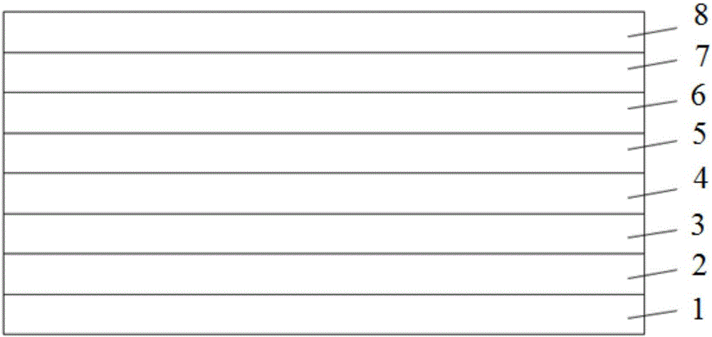
[0031] An embodiment of the present invention provides an epitaxial wafer of a gallium nitride-based light-emitting diode, see figure 1 , the epitaxial wafer includes a substrate 1, a buffer layer 2, an undoped GaN layer 3, an N-type GaN layer 4, a stress release layer 5, a multi-quantum well layer 6, and a P-type electron blocking layer sequentially stacked on the substrate 1. Layer 7, P-type GaN layer 8.

[0032] In this embodiment, the multi-quantum well layer 6 includes alternately stacked quantum well layers and quantum barrier layers. The quantum well layer is an InGaN layer; the quantum barrier layer is a GaN layer inserted with an InGaN layer, and the In composition content of the InGaN layer in the quantum barrier layer is lower than that of the InGaN layer in the quantum well layer.

[0033] Wherein, the In component content is the molar content of the In component.

[0034] Specifically, the stress release layer 5 includes alternately stacked InGaN layers and GaN ...

Embodiment 2

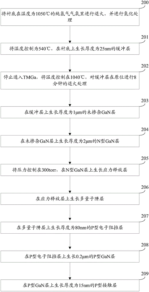
[0041] An embodiment of the present invention provides a method for manufacturing an epitaxial wafer of a gallium nitride-based light-emitting diode, which is suitable for manufacturing the epitaxial wafer of a gallium nitride-based light-emitting diode provided in Embodiment 1. Refer to figure 2 , the manufacturing method includes:

[0042] Step 200: annealing the substrate in a pure hydrogen atmosphere at a temperature of 1050° C., and performing nitriding treatment.

[0043] In this embodiment, with high-purity hydrogen (H 2 ) or nitrogen (N 2 ) as carrier gas, trimethylgallium (TMGa), trimethylaluminum (TMAl), trimethylindium (TMIn) and ammonia (NH3) as Ga, Al, In and N sources respectively, and silane (SiH4 ), two magnesium (CP2Mg) as N, P type dopant, respectively.

[0044] Step 201: Control the temperature to 540° C., and grow a buffer layer with a thickness of 25 nm on the substrate.

[0045] Step 202: Stop feeding TMGa, control the temperature at 1040° C., and pe...


PUM


Abstract

The present invention discloses a nitride-based luminous diode epitaxial wafer and a manufacturing method thereof, belonging to the field of the semiconductor technology. The epitaxial wafer comprises a substrate, a buffer layer stacked on the substrate in order, an un-doped GaN layer, a N-type GaN layer, a stress releasing layer, a multiple quantum well layer, a P-type electric barrier layer and a P-type GaN layer. The multiple quantum well layer includes a quantum well layer and a quantum barrier layer which are alternatively stacked, the quantum well layer is an InGaN layer, the quantum barrier layer is the GaN layer inserting the InGaN layer, and the In constituent content of the InGaN layer in the quantum well layer is lower than the In constituent content of the InGaN in the quantum well layer. The GaN quantum well layer inserts the InGaN layer having the In constituent content lower than the InGaN quantum well layer so as to improve the injection efficiency of the carrier, improve the effective recombination of the electrons and the hole in the quantum well and improve the quantum efficiency.

Description

technical field [0001] The invention relates to the technical field of semiconductors, in particular to an epitaxial wafer of a gallium nitride-based light-emitting diode and a manufacturing method thereof. Background technique [0002] Semiconductor light-emitting diodes (Light Emitting Diode, referred to as LED) have the advantages of high efficiency, energy saving, and environmental protection, and are widely used in fields such as traffic indication and outdoor full-color display. GaN-based materials include InGaN, GaN, AlGaN, and AlInGaN alloys, which have the advantages of large band gap, unsaturation of electron drift speed, strong breakdown field, small dielectric constant, good thermal conductivity, high temperature resistance, and corrosion resistance. Excellent material. [0003] The existing GaN-based LED epitaxial wafer includes a substrate, a buffer layer, an undoped GaN layer, an N-type GaN layer, a multi-quantum well layer, and a P-type GaN layer sequentiall...

Claims


Application Information

Patent Timeline
Patent Type & Authority Applications(China)
IPC IPC(8): H01L33/06H01L33/32H01L33/00
CPCH01L33/0075H01L33/06H01L33/325
Inventor 胡任浩郭炳磊吕蒙普胡加辉
Owner HC SEMITEK SUZHOU
Why Eureka
Try Eureka