Workpiece bonding system

A workpiece and bonding head technology, applied in electrical components, electrical solid devices, semiconductor devices, etc., can solve the problems of larger equipment size, increased equipment cost, low flexibility of preprocessing configuration, etc., to reduce transfer time, improve Production efficiency, the effect of saving production time

Inactive Publication Date: 2014-12-03
CETC BEIJING ELECTRONICS EQUIP
View PDF6 Cites 18 Cited by
  • Summary
  • Abstract
  • Description
  • Claims
  • Application Information

AI Technical Summary

Problems solved by technology

For example, in order to improve the efficiency of the whole machine on the basis of reliably completing chip preprocessing operations such as flipping, pre-alignment, and heating, some equipment sets up multiple independent preprocessing operation stations for parallel processing, but the cost is that the size of the equipment becomes larger and the preprocessing Configuration flexibility is not high
For another example, when it is necessary to remove the chip on the blue film and bond it to the wafer, due to the increasing size of the wafer (such as 300 mm), the equipment bonding head needs to change from The blue film pick-up position moves to the bonding position hundreds of millimeters away and then returns, which puts high requirements on the efficiency of the equipment and the reliability of motion control; some equipment manufacturers design two or more heads to overcome This problem, but the cost of equipment is greatly increased

Method used


Image

  • Workpiece bonding system
  • Workpiece bonding system
  • Workpiece bonding system

Examples


Embodiment Construction

[0068] In order to make the technical problems, technical solutions, and advantages to be solved by the embodiments of the present invention clearer, a detailed description will be given below with reference to the drawings and specific embodiments.

[0069] In view of the relatively low efficiency of the chip bonding equipment in the prior art, the embodiments of the present invention provide a workpiece bonding system, which uses a transfer method for the workpiece, and can also preprocess the workpiece during the transfer process. Reduce the time consumption of workpiece transfer and pretreatment, and improve the efficiency of workpiece bonding.

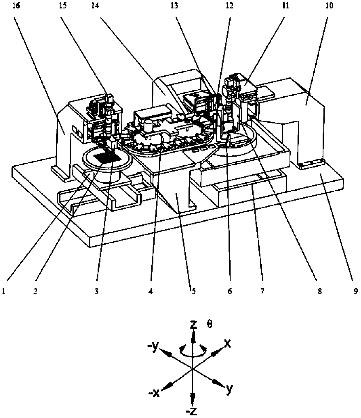
[0070] The embodiment of the present invention provides a workpiece bonding system, which includes a platen, a workpiece providing device provided on the platen, a workpiece conveying device, and a workpiece processing device, wherein,

[0071] The platen is used to support and fix each component of the entire workpiece bonding system;

...


PUM


Abstract

The invention provides a workpiece bonding system, and relates to the technical field of semiconductor processing and manufacturing. The workpiece bonding system is used for completing bonding processing of a semiconductor workpiece. The workpiece bonding system includes a workpiece providing device, a workpiece conveying device and a workpiece processing device. The workpiece providing device is used for obtaining a workpiece to be processed from a workpiece bearing device and conveying the workpiece to be processed to the workpiece conveying device; the workpiece conveying device is used for connecting the workpiece providing device and the workpiece processing device, obtaining the workpiece to be processed form the workpiece providing device, and conveying the workpiece to be processed to the workpiece processing device; and the workpiece processing device is used for obtaining the workpiece to be processed from the workpiece conveying device, and completing bonding of the workpiece. The workpiece conveying device can also be used for performing various preprocessing operation on the workpiece in the process of conveying the workpiece. The technical scheme of the workpiece bonding system in the invention can reduce consumption of time for workpiece delivery and preprocessing, and improve the overall efficiency of workpiece bonding.

Description

Technical field [0001] The invention relates to the technical field of semiconductor processing and manufacturing, in particular to a workpiece bonding system. Background technique [0002] Chip bonding is an indispensable key process step in the semiconductor device packaging process. The diced bare chip adhered to the blue film must undergo a series of processes such as bonding and plastic packaging to form a usable semiconductor device. Different semiconductor devices and their corresponding chips may require different chip bonding processes. For example, some chips require eutectic bonding and others require die bond bonding; some chips need to be removed from the blue film and flipped and then bonded while other chips do not need to be flipped; some chips will be bonded to the lead frame Or on the substrate and other chips will be bonded to the wafer; some chips need to be heated before bonding while other chip bonding is performed at room temperature; some chips need to be...

Claims


Application Information

Patent Timeline
Patent Type & Authority Applications(China)
IPC IPC(8): H01L21/677H01L21/687H01L21/60
CPCH01L21/67703H01L21/67718H01L24/80H01L2224/80
Inventor 唐亮郎平周启舟郝术壮么文静
Owner CETC BEIJING ELECTRONICS EQUIP
Why Eureka
Try Eureka