


Quick Research
Generate reliable direction feasibility study reports for your R&D in just a few steps.

Technical Q&A
Discover and master advanced knowledge NOW. Basics, ideas, possibilities, all at once.

Find Solutions
As an expert in R&D theories, this can generate solutions to your technical problems instantly.

Evaluate Feasibility
Analyze your overall solution with one click, know your potential R&D risks in advance.

Monitor Landscape
Get weekly tech updates, stay abreast of the latest tech innovations and key insights.
Nitride semiconductor device
一种氮化物半导体、器件的技术,应用在半导体器件、半导体/固态器件制造、电固体器件等方向,能够解决低接触电阻、欧姆电极接触电阻高等问题,达到接触电阻降低的效果
- Summary
- Abstract
- Description
- Claims
- Application Information
AI Technical Summary
Problems solved by technology
Method used
Image

Examples
no. 1 approach
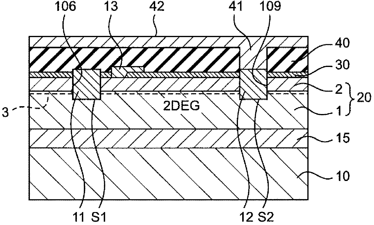
[0071] figure 1 A cross-sectional view showing a nitride semiconductor device according to a first embodiment of the present invention, which is a GaN-based HFET (Hetero-junction Field Effect Transistor: heterojunction field effect transistor).
[0072] The semiconductor device, such as figure 1 As shown, an undoped AlGaN buffer layer 15 and a nitride semiconductor stacked body 20 including undoped AlGaN as an example of a first nitride semiconductor layer are formed on a Si substrate 10. GaN layer 1 and undoped AlGaN layer 2 as an example of the second nitride semiconductor layer. The interface between the undoped GaN layer 1 and the undoped AlGaN layer 2 is a heterointerface. A 2DEG layer (two-dimensional electron gas layer) 3 is generated near the interface between the undoped GaN layer 1 and the undoped AlGaN layer 2 .
[0073] In addition, instead of the GaN layer 1 described above, an AlGaN layer having a composition having a band gap smaller than that of the AlGaN la...
no. 2 approach
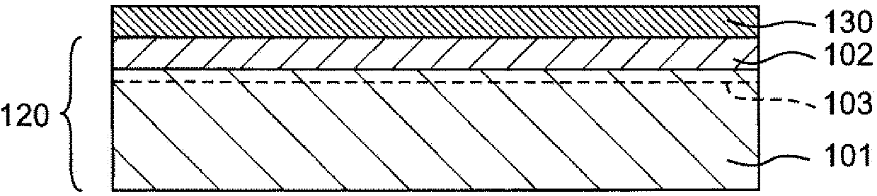
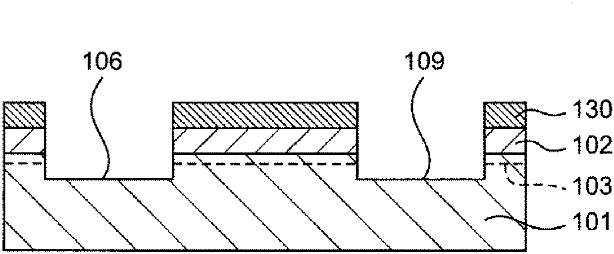
[0120] Figure 11 A cross-sectional view showing a nitride semiconductor device according to a second embodiment of the present invention, which is a GaN-based HFET (Hetero-junction Field Effect Transistor: heterojunction field effect transistor).
[0121] In addition, in the description of the nitride semiconductor device of the second embodiment, the same reference numerals as those of the constituent elements of the first embodiment are assigned to the same constituent elements as those of the nitride semiconductor device of the first embodiment. Numbers are used for brief explanations, and detailed descriptions are omitted.
[0122] The semiconductor device, such as Figure 11 As shown, an undoped AlGaN buffer layer 15 and a nitride semiconductor stacked body 220 including undoped AlGaN as an example of a first nitride semiconductor layer are formed on a Si substrate 10. GaN layer 201 and undoped AlGaN layer 202 as an example of the second nitride semiconductor layer. T...
PUM
 Abstract
Description
Claims
Application Information
 - R&D Engineer
- R&D Manager
- IP Professional
- Industry Leading Data Capabilities
- Powerful AI technology
- Patent DNA Extraction
Browse by: Latest US Patents, China's latest patents, Technical Efficacy Thesaurus, Application Domain, Technology Topic, Popular Technical Reports.
© 2024 PatSnap. All rights reserved.Legal|Privacy policy|Modern Slavery Act Transparency Statement|Sitemap|About US| Contact US: help@patsnap.com