Array substrate, preparation method of array substrate and display device
An array substrate and substrate technology, which is applied in semiconductor/solid-state device manufacturing, optics, instruments, etc., can solve the problems of affecting voltage uniformity, high resistance, and affecting the uniformity of alignment film, so as to improve aperture ratio, ensure uniformity, The effect of reducing the total resistance
- Summary
- Abstract
- Description
- Claims
- Application Information
AI Technical Summary
Problems solved by technology
Method used
Image

Examples
Embodiment 1
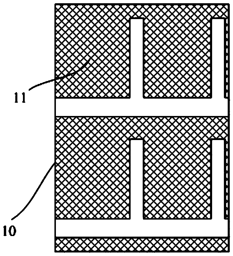
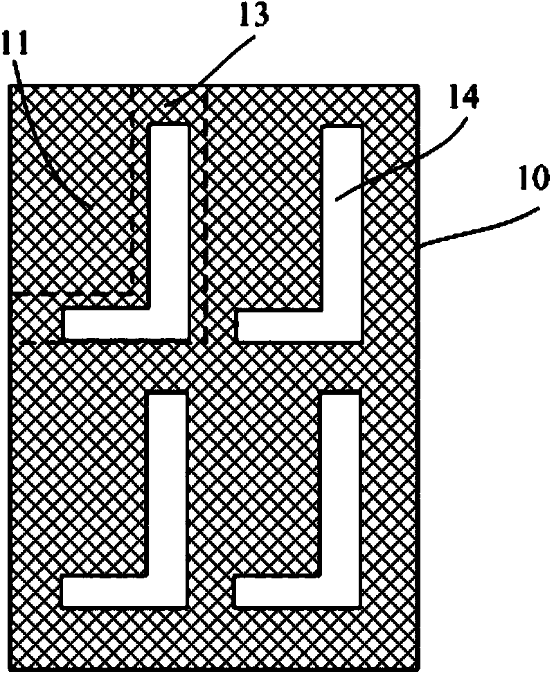
[0035] to combine Figures 3 to 5 As shown, this embodiment provides an array substrate, which includes a substrate, a common electrode layer 10, a first insulating layer 50, and a gate layer sequentially arranged on the substrate; wherein, the common electrode layer 10 includes a The plurality of corresponding common electrodes 11 and the common electrode connecting portion 13, each of the common electrodes 11 is connected through the common electrode connecting portion 13; the gate line layer is electrically insulated from the common electrode layer 10 through the first insulating layer 50 open.
[0036] It should be noted that the common electrode 11 and the common electrode connecting portion 13 can be connected as a complete surface structure, that is to say, the common electrode 11 and the common electrode connecting portion 13 are only different in area distribution and function, and the materials of the two The same, of course, the common electrode connecting portion ...
Embodiment 2
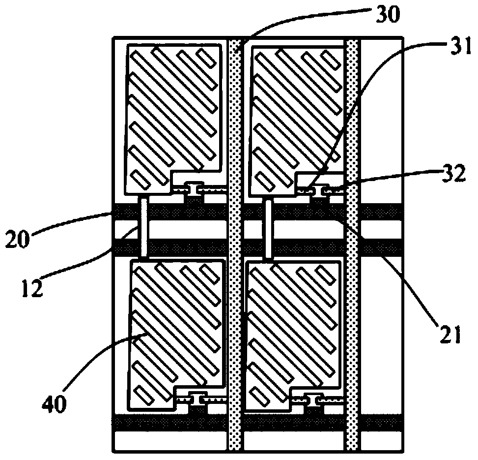
[0039] to combine Figures 3 to 5 As shown, this embodiment provides an array substrate, which is based on the array substrate in Embodiment 1, and the array substrate in this embodiment further includes elements such as thin film transistors and data line layers. In order to describe the structure of the array substrate in this embodiment more clearly, the following describes an array substrate including bottom-gate TFTs as an example, but the types of TFTs are not limited to bottom-gate TFTs, and top-gate TFTs are also feasible. , will not be described in detail here.
[0040] The array substrate in this embodiment includes: a base;
[0041] A common electrode layer 10 disposed on the substrate, wherein a plurality of L-shaped openings 14 for defining each of the common electrodes are disposed in the common electrode connection portion of the common electrode layer; the first insulating layer disposed on the common electrode layer 50, wherein a common electrode contact reg...
Embodiment 3
[0049] This embodiment provides a method for preparing an array substrate. The array substrate may be the array substrate described in Embodiment 1 or 2, and the steps specifically include:
[0050] Step 1. Form a pattern including a common electrode layer on the substrate through a patterning process. The common electrode layer includes a plurality of common electrodes corresponding to each pixel area and a common electrode connecting portion, and each of the common electrodes is connected through the common electrode. department connection.
[0051] It should be noted that the common electrode and the common electrode connection part can be connected as a complete surface structure, that is to say, the common electrode and the common electrode connection part are only different in area distribution and function, and the materials of the two are the same. Of course, the common electrode connection part may also have a structure with openings, but it only needs to ensure the e...
PUM
 Abstract
Description
Claims
Application Information
 - Generate Ideas
- Intellectual Property
- Life Sciences
- Materials
- Tech Scout
- Unparalleled Data Quality
- Higher Quality Content
- 60% Fewer Hallucinations
Browse by: Latest US Patents, China's latest patents, Technical Efficacy Thesaurus, Application Domain, Technology Topic, Popular Technical Reports.
© 2025 PatSnap. All rights reserved.Legal|Privacy policy|Modern Slavery Act Transparency Statement|Sitemap|About US| Contact US: help@patsnap.com