Organic light-emitting device and manufacturing method thereof

A technology of organic light-emitting devices and organic light-emitting elements, which is applied in the field of OLED displays, can solve the problems of reduced device efficiency and lifespan, high cost of single-chip heat sinks, heat accumulation, etc., to achieve enhanced brightness, beneficial heat dissipation, and enhanced heat dissipation effects Effect

Inactive Publication Date: 2014-12-10
EVERDISPLAY OPTRONICS (SHANGHAI) CO LTD
View PDF6 Cites 29 Cited by
  • Summary
  • Abstract
  • Description
  • Claims
  • Application Information

AI Technical Summary

Problems solved by technology

[0003] In addition, because sometimes OLED display modules have long-term display requirements in a certain area, heat accumulation will inevitably occur, which will reduce the efficiency and life of some devices
For the uniformity of heat, at p

Method used


Image

  • Organic light-emitting device and manufacturing method thereof
  • Organic light-emitting device and manufacturing method thereof
  • Organic light-emitting device and manufacturing method thereof

Examples


Example Embodiment

[0044] The present invention will be described in detail below with reference to the specific embodiments shown in the accompanying drawings. However, these embodiments do not limit the present invention, and structural, method, or functional changes made by those skilled in the art according to these embodiments are all included in the protection scope of the present invention.

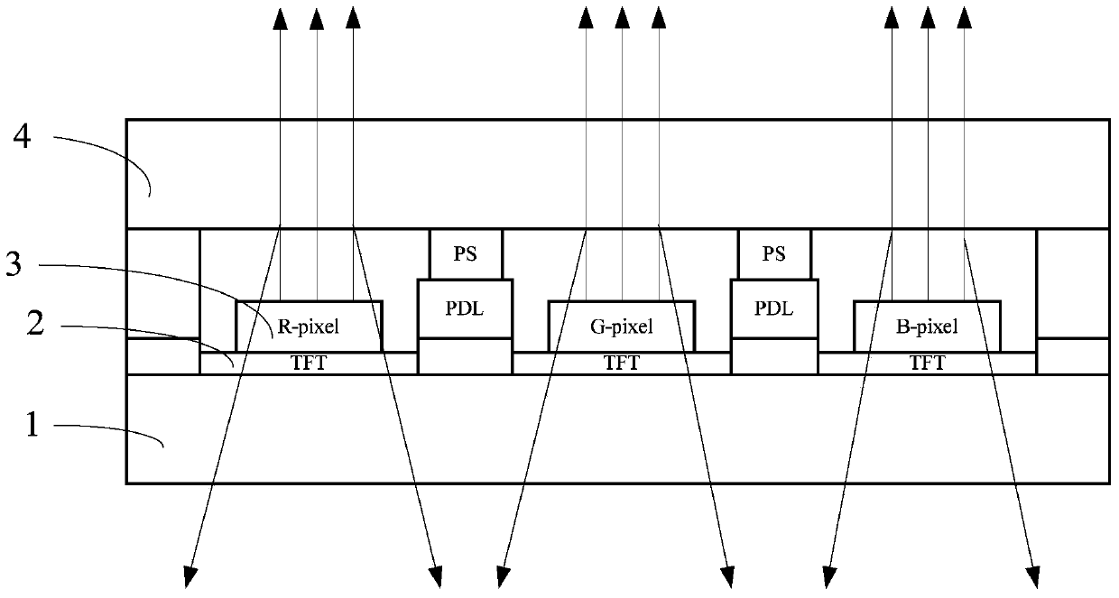
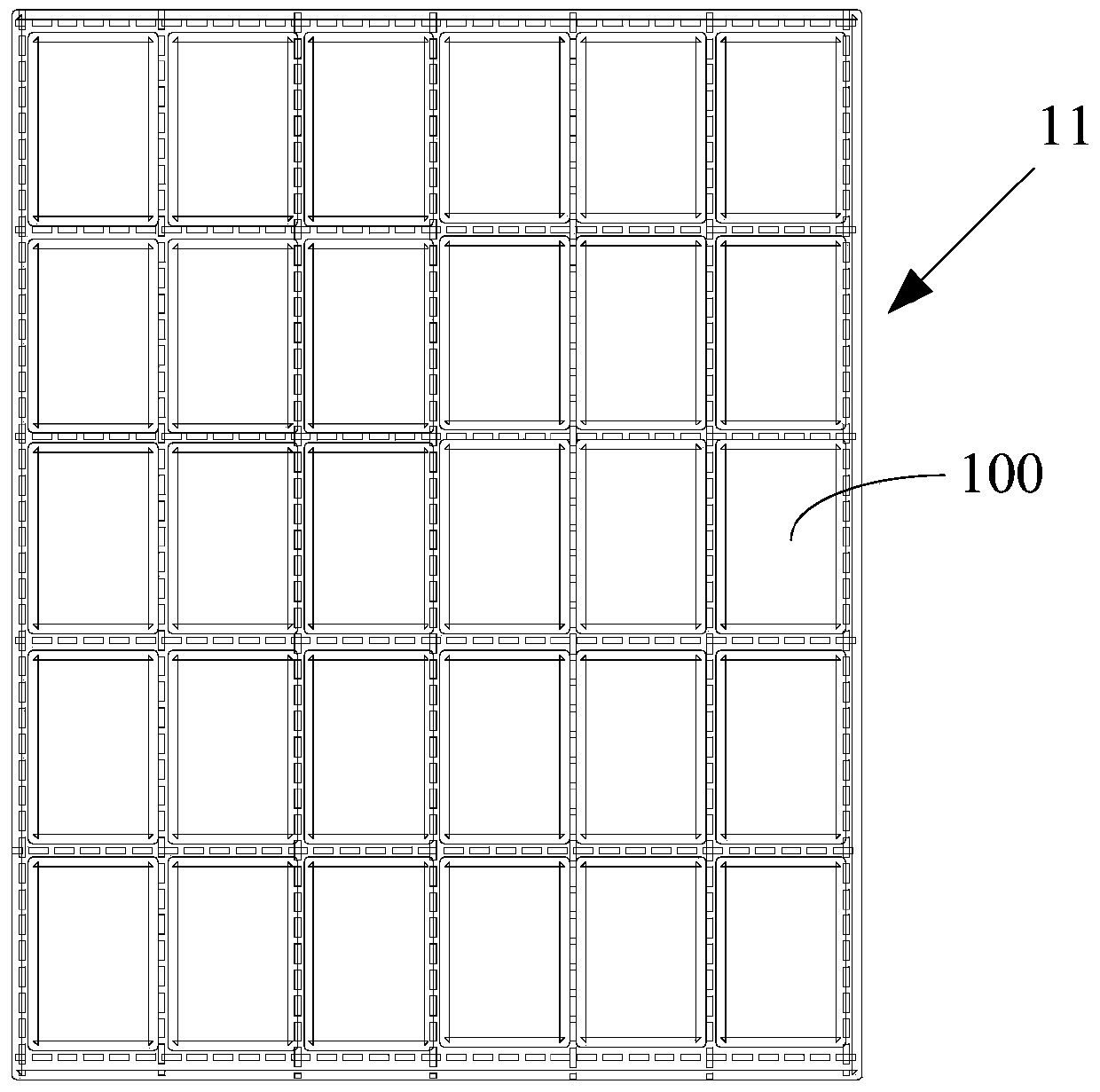
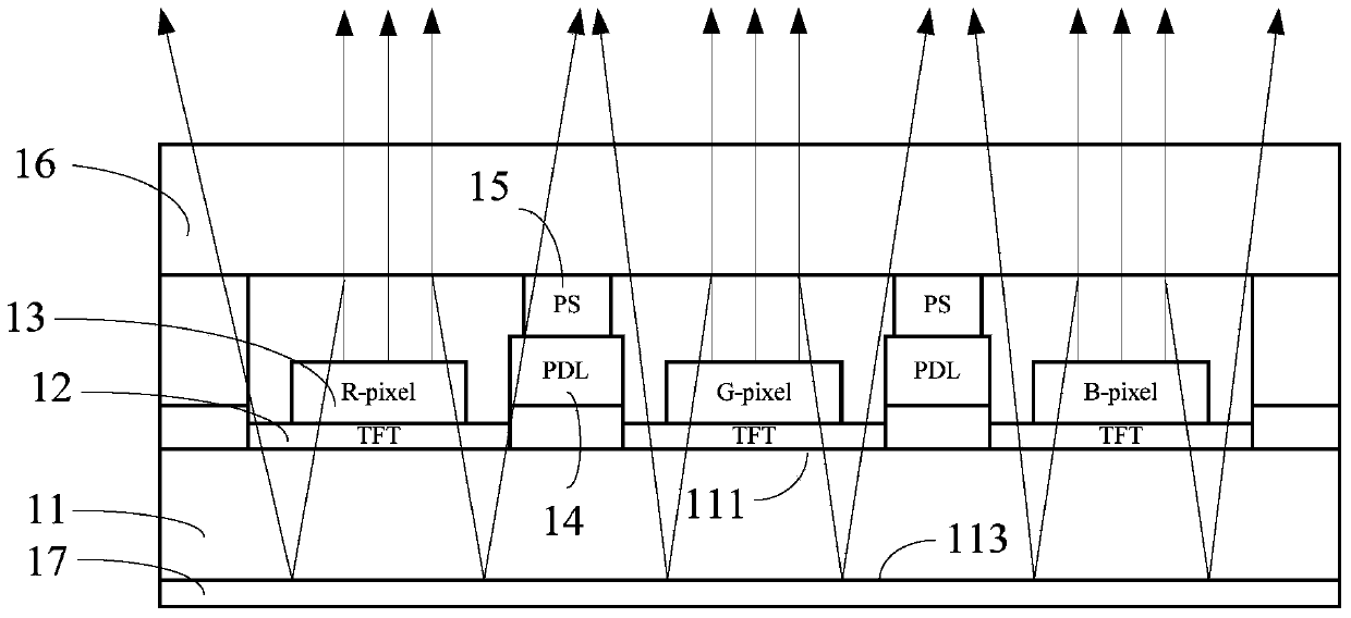
[0045] Please refer to figure 2 and image 3 , figure 2 It is a schematic structural diagram of a plurality of organic light-emitting devices on the transparent substrate of the present invention; image 3 It is a schematic cross-sectional structure diagram of the organic light-emitting device of the present invention. The organic light emitting device of the present invention includes: a transparent substrate 11 , a light emitting unit 13 , a thin film transistor 12 , a pixel definition layer 14 , a spacer 15 , a package cover 16 and a metal reflection layer 17 . The transparent substrate 11 i...


PUM

PropertyMeasurementUnit
Thicknessaaaaaaaaaa

Abstract

The invention discloses an organic light-emitting device. The organic light-emitting device comprises a transparent substrate including a first face and a second face opposite to the first face, multiple light-emitting units located on the first face of the transparent substrate, a thin film transistor arranged on the transparent substrate and located between the first face and the light-emitting units, a pixel definition layer arranged between any two adjacent light-emitting units, a packaging cover plate sealing the thin film transistor, the light-emitting units and the pixel definition layer between the packaging cover plate and the transparent substrate, a partition part arranged on the pixel definition layer, sealed between the packaging cover plate and the transparent substrate and used for supporting the packaging cover plate and a metal reflection layer arranged on the second face. The invention further provides a manufacturing method of the organic light-emitting device. The metal reflection layer is arranged on the back face of the transparent substrate to improve the light emergence efficiency of an OLED device and strengthen the brightness of an OLED display module and meanwhile facilitates heat loss of a display module, and reduction of the light-emitting efficiency of the device and shortening of the service life of the device due to heat accumulation are avoided.

Description

technical field [0001] The invention relates to the technical field of OLED displays, in particular to an organic light-emitting device and a preparation method thereof. Background technique [0002] As a new generation of display devices, organic electroluminescent devices (OLEDs) have many advantages, and have broad application prospects in mobile phones, digital cameras, vehicle displays, notebook computers and military fields. Such as figure 1 As shown, the OLED display generally adopts a glass substrate 1, and a transistor device 2, a light-emitting unit 3, and a package cover 4 are sequentially formed on the glass substrate 1, wherein the transistor device 2 of the driving backplane of the OLED display adopts a translucent Therefore, the following situation will inevitably occur. After testing, about 18%-20% of the light will be transmitted to the back of the glass substrate 1 through the light-transmitting material due to the reflection of each interface, and then be...

Claims


Application Information

Patent Timeline
IPC IPC(8): H01L27/32H01L51/52H01L51/56
Inventor 张其国温志伟宋楠楠
Owner EVERDISPLAY OPTRONICS (SHANGHAI) CO LTD
Why Eureka
Try Eureka