Delay method and delay circuit for input under-voltage protection circuit

A protection circuit, input undervoltage technology, applied in the field of control chips with input undervoltage protection circuit, can solve the problems of power supply impact, power supply output voltage rise, not meeting power supply performance index requirements, etc., to achieve the effect of avoiding failure

Active Publication Date: 2014-12-10
MORNSUN GUANGZHOU SCI & TECH
View PDF6 Cites 3 Cited by
  • Summary
  • Abstract
  • Description
  • Claims
  • Application Information

AI Technical Summary

Problems solved by technology

[0005] But to do a delay circuit, when the chip is started or the module is reset, the capacitor, D flip-flop, counter, etc. must be initialized inside the chip, and because when the chip is started or the module is reset, it is necessary to ensure that the chip works normally and does not enter any protection state, so it must be initialized to the non-input undervoltage state, but initialized to the non-input undervoltage state, there will be a problem: if image 3 In the timing diagram shown, ENP_lv represents the low-voltage module initialization signal, which is high after initialization; VIN_fault_L represents the input undervoltage detection signal, which is active at low level; UVIN_L represents the undervoltage protection control signal, which is active at low level; GATE is the output pulse Signal
But during this period, once the input voltage is lower than the set undervoltage point, the input voltage Vin

Method used


Image

  • Delay method and delay circuit for input under-voltage protection circuit
  • Delay method and delay circuit for input under-voltage protection circuit
  • Delay method and delay circuit for input under-voltage protection circuit

Examples


Embodiment 1

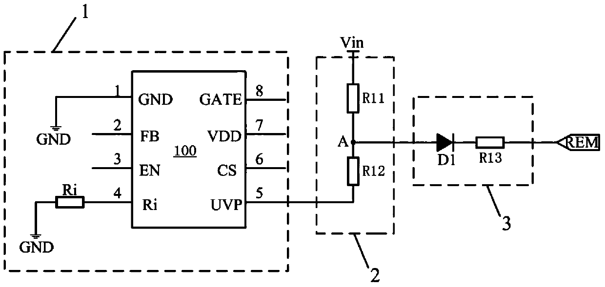
[0027] Such as Figure 4 Shown is the circuit diagram of Embodiment 1 of the present invention. A delay circuit of an input undervoltage protection circuit generated by the change of the FB terminal voltage VFB, including a sampling voltage establishment module and a pulse output control module. The sampling voltage establishment module has an FB terminal (also known as an output voltage feedback terminal, hereinafter collectively referred to as FB terminal) and SS terminal (also known as soft start terminal, hereinafter referred to as SS terminal), the pulse output control module has GATE terminal (also known as pulse output terminal, hereinafter referred to as GATE terminal),

[0028]The sampling voltage building module, when the SS terminal voltage Vss rises slowly, when the SS terminal voltage Vss rises to the conduction voltage Vbe2 of the transistor Q2, the transistor Q2 is turned on, and the output terminal voltage of the operational amplifier AMP2 follows its positive ...

Embodiment 2

[0057] Such as Figure 5 As shown, compared with Embodiment 1, the difference of the delay circuit of the input undervoltage protection circuit in this embodiment is that in the sampling voltage establishment module 201, the triode Q2 is removed, that is, the sampling voltage establishment module includes: current source Iss, The power supply terminal VCCA, transistor Q1, operational amplifier AMP2, resistors R1, R2 and R3, the output terminal of the current source Iss are respectively connected to the SS terminal and the positive input terminal of the operational amplifier AMP2, and the negative input terminals of the operational amplifier AMP2 are respectively connected to the operational amplifier The output terminal of AMP2 is connected to the FB terminal, the output terminal of the operational amplifier AMP2 is also connected to the base of the transistor Q1, the collector of the transistor Q1 is short-circuited to the base, and the collector of the transistor Q1 is also c...


PUM


Abstract

The invention aims to provide a delay circuit for an input under-voltage protection circuit. The delay circuit comprises a sampling voltage setup module and a pulse output control module. The sampling voltage setup module sets up a sampling voltage Vp by enabling a voltage VFB of an output voltage feedback end to follow up a voltage Vss of a soft starting end; the pulse output control module receives the sampling voltage Vp and compares the sampling voltage Vp with a set value prior to outputting signals to control on/off of a GATE end. The delay circuit for the input under-voltage protection circuit has the advantages that before finishing of soft starting and after arrival of under-voltage protection signals, the GATE end is free of output, and accordingly an output voltage of a power source cannot rise instantly, and influences on post-stage circuits due to false triggering can be avoided.

Description

technical field [0001] The invention relates to an integrated circuit, in particular to a control chip with an input undervoltage protection circuit. Background technique [0002] The Chinese invention patent application published on August 13, 2014 with the publication number CN103986320 discloses a switching power supply remote control circuit, which has an undervoltage protection function, such as figure 1 As shown, it includes switching power supply control circuit 1, voltage sampling circuit 2 and remote control port circuit 3. Among them, the switching power supply control circuit 1 includes a control IC, which is an existing switching power supply control chip, which can output driving pulses with a certain frequency and a certain duty ratio according to the state of the circuit. The chip has an undervoltage protection function and is The undervoltage protection function is realized by detecting the input current of the undervoltage protection terminal UVP. [0003]...

Claims


Application Information

Patent Timeline
Patent Type & Authority Applications(China)
IPC IPC(8): H02M1/36H02M1/32
Inventor 唐盛斌赵志伟符威
Owner MORNSUN GUANGZHOU SCI & TECH
Why Eureka
Try Eureka