PCB and wiring method thereof

A wiring method and signal line technology, applied in printed circuit components, electrical components, printed circuit manufacturing, etc., can solve problems such as crosstalk electromagnetics and interference, and achieve the goals of reducing electromagnetic radiation, enhancing stability, and reducing loop area Effect

Inactive Publication Date: 2014-12-10
INSPUR BEIJING ELECTRONICS INFORMATION IND
View PDF10 Cites 9 Cited by
  • Summary
  • Abstract
  • Description
  • Claims
  • Application Information

AI Technical Summary

Problems solved by technology

[0005] The invention provides a PCB and its wiring method to solve the

Method used


Image

  • PCB and wiring method thereof
  • PCB and wiring method thereof
  • PCB and wiring method thereof

Examples


Example Embodiment

[0027] The technical solutions in the embodiments of the present invention will be clearly and completely described below in conjunction with the accompanying drawings in the embodiments of the present invention. Obviously, the described embodiments are only a part of the embodiments of the present invention, rather than all the embodiments. Based on the embodiments of the present invention, all other embodiments obtained by those of ordinary skill in the art without creative work shall fall within the protection scope of the present invention.

[0028] It should be noted that, if there is no conflict, the embodiments of the present invention and various features in the embodiments can be combined with each other, and all fall within the protection scope of the present invention. In addition, although a logical sequence is shown in the flowchart, in some cases, the steps shown or described may be performed in a different order than here.

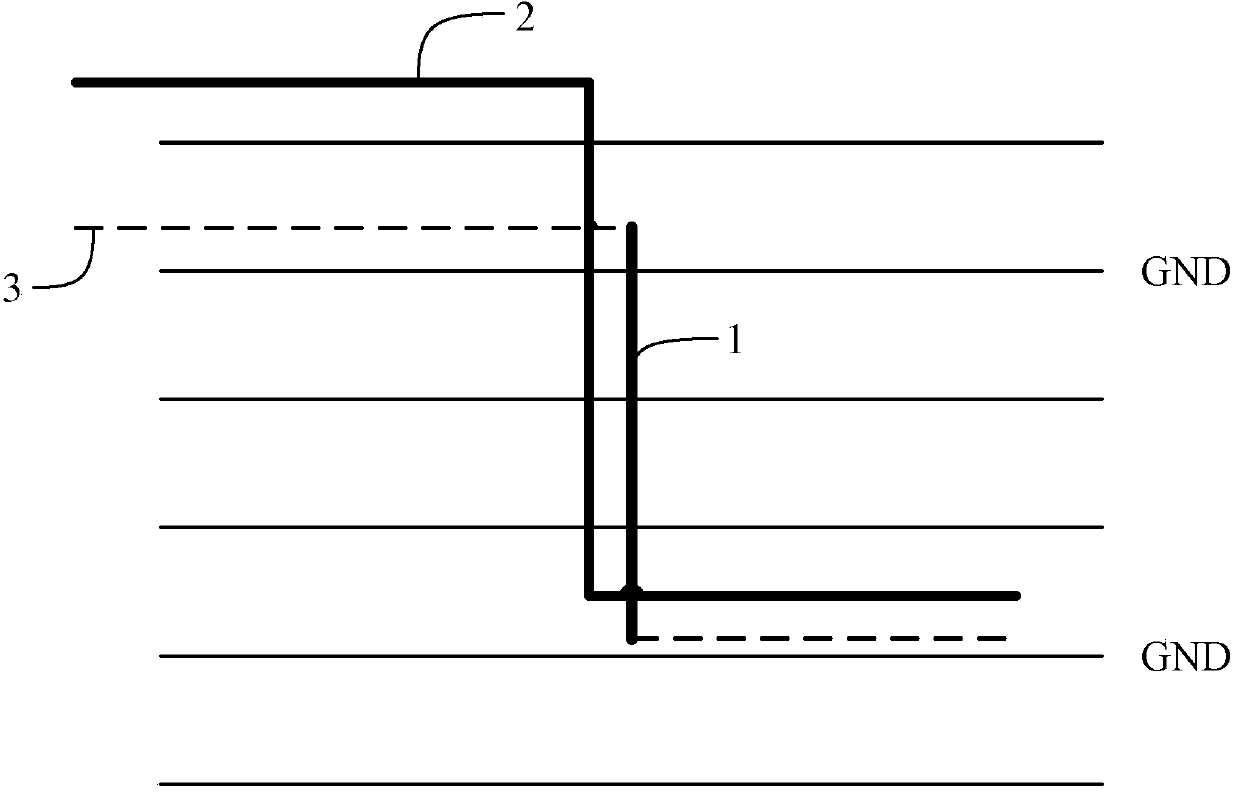
[0029] In the PCB, the return current of t...


PUM


Abstract

The invention discloses a PCB and wiring method thereof. The method comprises the following steps: accompanying ground holes are additionally formed near layer changing through holes, and are wrapped in the middle of signal wires. According to the invention, as the accompanying ground holes are additionally formed, the signal wires and the accompanying ground holes form a signal loop circuit; the problem that reversed flow ground plane is missing is solved; a favorable reversed flow track is provided for signals; convenience is provided for nearby reversed flow after the signals change layer; loop circuit area is reduced; electromagnetic radiation caused by layer changing of the signals is reduced, so that the signal quality and stability of a system are improved.

Description

technical field [0001] The invention relates to the field of printed circuit boards, in particular to a PCB and a wiring method thereof. Background technique [0002] With the increasing maturity of mobile communication technology, the transmission rate of wireless signals is gradually increasing, and the functions and integration of wireless terminals are also increasing. The rise time and fall time of the signal are also continuously shortened, and the signal integrity plays an increasingly important role in the effective transmission of the signal. [0003] In the prior art, a PCB usually has 6-8 signal layers. Ideally, the signal lines should be routed on the same layer in the PCB, and each signal layer is adjacent to a complete reference ground plane, and the return current of the signal flows in the adjacent ground plane. According to the skin effect, about 95% of the return current will flow down the central strip region of the trace, and the other 5% will be distri...

Claims


Application Information

Patent Timeline
IPC IPC(8): H05K1/02H05K3/00
Inventor 王素华龚艳鸿张柯柯
Owner INSPUR BEIJING ELECTRONICS INFORMATION IND
Why Eureka
Try Eureka