Conductive ink composition, method for producing conductive patterns, and conductive circuit

A technology of conductive ink and composition, which is applied to the formation of conductive patterns, equipment for manufacturing conductive/semiconductive layers, conductive materials dispersed in non-conductive inorganic materials, etc., which can solve the problem of high curing temperature and long firing time and other issues to achieve high productivity

Active Publication Date: 2014-12-10
DIC CORP
View PDF7 Cites 3 Cited by
  • Summary
  • Abstract
  • Description
  • Claims
  • Application Information

AI Technical Summary

Problems solved by technology

However, there are the following disadvantages: the calcination temperature is 150°C, the curing temperature is high because it does not contain an isocyanate reaction catalyst, and the calcination time is long because the isocyanate blocking agent is MEK oxime
This technology also has the following problems in the same way as the technology of the above-mentioned Patent Document 1: the roasting condition is 130° C. for 30 minutes, the roasting time is long because no isocyanate reaction catalyst is added, and the roasting time is long because the isocyanate blocking agent is MEK oxime

Method used


Image

  • Conductive ink composition, method for producing conductive patterns, and conductive circuit
  • Conductive ink composition, method for producing conductive patterns, and conductive circuit

Examples


Embodiment

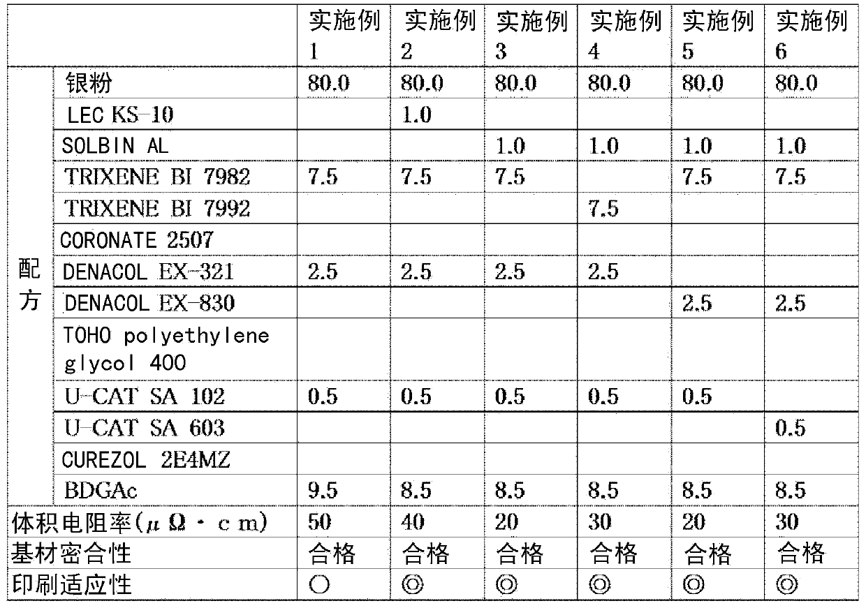
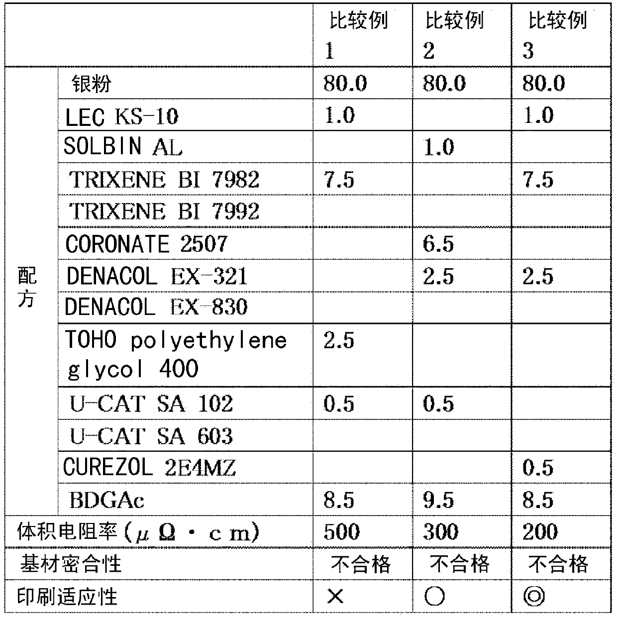
[0067] Hereinafter, the present invention will be specifically described based on examples. "%" here means "mass %" unless otherwise specified.

[0068] Each raw material was used in parts by mass described in Table 1, and these raw materials were mixed sufficiently to prepare each conductive ink composition of the present invention as an example and each conventional conductive ink composition as a comparative example.

[0069] For each of these conductive ink compositions, the characteristics of the conductive ink composition itself and the characteristics of the conductive pattern obtained therefrom were evaluated by the following measurement items. The evaluation results are collectively shown in Table 1 and Table 2 below.

[0070](volume resistivity)


PUM

PropertyMeasurementUnit
particle sizeaaaaaaaaaa
particle diameteraaaaaaaaaa
boiling pointaaaaaaaaaa

Abstract

[Problem] To provide a conductive ink composition that enables extremely fine conductive patterns to be formed, and that enables high conductivity patterns, which can be fired at a lower temperature and in a shorter time, to be obtained. [Solution] The abovementioned problem is solved by including, as essential components, a conductive filler, an epoxy compound, a blocked polyisocyanate, which is a blocking agent comprising an active methylene compound and / or a pyrazole compound, and an organic solvent and reaction catalyst for the blocked polyisocyanate. This conductive ink composition can be fired at a lower temperature and in a shorter time, and enables finer conductive patterns to be printed.

Description

technical field [0001] The present invention relates to a conductive ink composition for forming a conductive film, a method for producing a conductive pattern, and a conductive circuit. Background technique [0002] A printing method or an etching method is known as a method for forming conductive patterns such as conductive circuits and electrodes used in touch panels, electronic paper, and various electronic components. [0003] When forming a conductive pattern by etching, it is necessary to form a resist film patterned by photolithography on the substrate on which various metal films are deposited, and then dissolve and remove unnecessary deposited metal films chemically or electrochemically. , and finally remove the resist film, the process is very complicated and lacks mass production. [0004] On the other hand, the printing method can mass-produce a desired pattern at low cost, and can also easily impart conductivity by drying or curing a printed coating film. [...

Claims


Application Information

Patent Timeline
Patent Type & Authority Applications(China)
IPC IPC(8): C09D11/52H01B1/00H01B1/22H01B5/14H01B13/00H05K1/09H05K3/12
CPCH05K3/1216H05K3/1275C09D11/037H01B1/22H05K1/092C09D11/102C09D11/52H01B13/0026H05K1/095H05K1/097
Inventor 冈本朋子千手康弘片山嘉则
Owner DIC CORP
Why Eureka
Try Eureka