Method of fabrication of micro-optics device with curved surface defects

A manufacturing method and technology for curved surfaces, applied in optical elements, photoengraving process of pattern surface, optics, etc., can solve the problem of SPL probe being in the development stage, etc.

Active Publication Date: 2014-12-10
IBM CORP
View PDF7 Cites 6 Cited by
  • Summary
  • Abstract
  • Description
  • Claims
  • Application Information

AI Technical Summary

Problems solved by technology

However, the use of SPL probes for nanopatterning applications is still under development

Method used


Image

  • Method of fabrication of micro-optics device with curved surface defects
  • Method of fabrication of micro-optics device with curved surface defects
  • Method of fabrication of micro-optics device with curved surface defects

Examples


Embodiment Construction

[0058] The description below is structured as follows:

[0059] I. Introduction

[0060] II. Description of Vertical Microcavity

[0061] III. Manufacturing method

[0062] IV. Final Considerations

[0063] I. Introduction

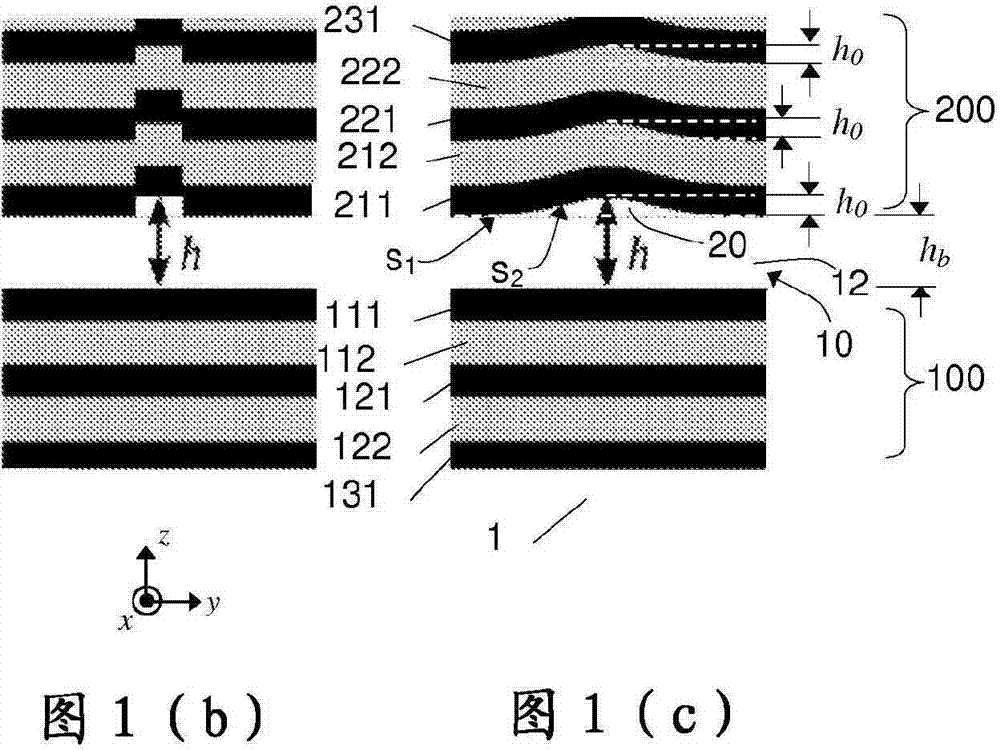
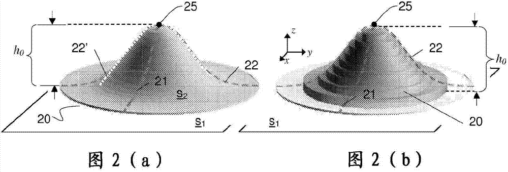
[0064] The present invention uses novel nanopatterning techniques to accurately pattern "defects" embedded in micro-optical devices such as microcavities. Defects can be given a specific, precise and smooth profile (or shape) that allows increased interaction with electromagnetic waves, eg for electromagnetic wave confinement applications. Furthermore, embedded defects can have well-controlled curvatures (eg, faithful Gaussian shapes) at adjacent vertices, leading to unprecedented constraint properties. Such curved defect shapes are not achievable with existing techniques such as evaporation or planar etching. The fabrication method considered here involves a modified SPL technique in which polymer chains are desorbed or unchained to a fine particle ...


PUM

PropertyMeasurementUnit
molecular weightaaaaaaaaaa

Abstract

A method of fabrication of a micro-optics device included providing a layer of material; patterning the layer of material by one or more of: locally unzipping and desorbing molecules thereof, with a nano-scale dimensioned probe, to obtain a curved surface for the layer of material, the curved surface having a curved profile in a plane section; and completing a layer structure perpendicular to the plane section by providing one or more additional layers of material in contact with the curved surface to obtain the micro-optics device, wherein the micro-optics device has the layer structure, with a given layer thereof comprising a defect delimited by two surfaces, wherein one of the two surfaces is the curved surface.

Description

technical field [0001] The present invention generally relates to methods of fabricating micro-optical devices, such as vertical microcavities. More specifically, it relates to methods of manufacturing micro-optical components with embedded defects for enhanced electromagnetic wave confinement. Background technique [0002] Micro-optics such as optical microcavities are known to confine light into small volumes. Today's devices using optical microcavities are essential in many fields ranging from optoelectronics to quantum information. Typical applications are long-distance data transmission over optical fibers and read / write laser beams in DVD / CD players. A variety of confined semiconductor microstructures have been developed and investigated, involving various geometries and resonant properties. A "microcavity" (hereinafter MC) has smaller dimensions than conventional optical cavities; its dimensions are often only a few micrometers and they include parts that can even ...

Claims


Application Information

Patent Timeline
Patent Type & Authority Applications(China)
IPC IPC(8): G03F7/00
CPCH01S5/18388G02B5/284H01S5/18391Y10T428/24736H01S5/18308H01S5/2004H01S5/2054G03F7/0002G02B5/288H01L33/10G02B5/0816
Inventor 丁飞U·T·迪里希A·W·科诺尔R·F·马特T·H·斯托福尔
Owner IBM CORP
Why Eureka
Try Eureka