Sealing rings and chip with same

A sealing ring and inner sealing ring technology, which is applied in the direction of electrical components, electric solid devices, circuits, etc., can solve the problem that the stress cannot be prevented from spreading to the integrated circuit area of ​​the chip

Active Publication Date: 2014-12-17
SEMICON MFG INT (SHANGHAI) CORP
View PDF4 Cites 0 Cited by
  • Summary
  • Abstract
  • Description
  • Claims
  • Application Information

AI Technical Summary

Problems solved by technology

[0008] The problem solved by the present invention is that the sealing ring formed in the chip in the prior art still has the risk of being unable to prevent the stress from propagating to the integrated circuit area of ​​the chip, causing cracks and peeling to spread to the integrated circuit area

Method used


Image

  • Sealing rings and chip with same
  • Sealing rings and chip with same
  • Sealing rings and chip with same

Examples


no. 1 example

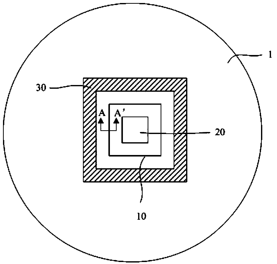
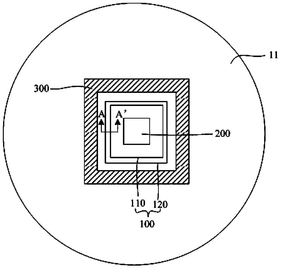
[0040] refer to image 3 , image 3It is a top view of the chip sealing ring 100 , the integrated circuit area 200 and the dicing line 300 formed on the wafer 11 . The chip sealing ring 100 is surrounded by a dicing line 300 , and the chip sealing ring 100 surrounds an integrated circuit region 200 in the chip. The chip sealing ring 100 includes an inner sealing ring 110 and an outer sealing ring 120 surrounding the inner sealing ring 110 . That is, the inner sealing ring 110 is closer to the integrated circuit area 200 .

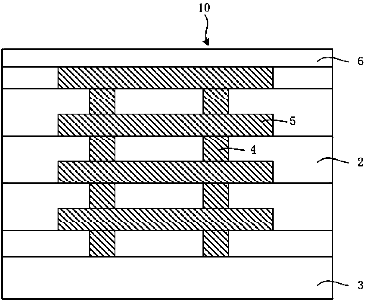
[0041] refer to Figure 4 , Figure 4 for image 3 Schematic diagram of the plane cut along the tangent AA'. The chip sealing ring 100 is located in the dielectric layer 130 of the chip, and the dielectric layer 130 and the integrated circuit region 200 are both located on the substrate 101 . The dicing line 300 is located on the left side of the chip sealing ring 100 , and the right side of the chip sealing ring 100 is the integrated circuit area 20...

no. 2 example

[0057] refer to Figure 5 , In a specific embodiment, the number of the inner sealing ring or the outer sealing ring is more than two, or the number of the inner sealing ring and the outer sealing ring is more than two. Figure 5 Shown are outer seal ring 120A and outer seal ring 120B, inner seal ring 110A and inner seal ring 110B.

[0058] In a specific embodiment, the number of the inner sealing ring and the outer sealing ring is more than two, the material of each first plug in the inner sealing ring is the same, and the inner sealing ring near the integrated circuit area The diameter of the first plug is larger than the diameter of the first plug in the inner seal ring away from the integrated circuit area; or, the diameters of each first plug are the same, and the first plug material in the inner seal ring near the integrated circuit area The fracture toughness is greater than the fracture toughness of the first plug material in the inner sealing ring far away from the i...

no. 3 example

[0064] refer to Image 6 , in a specific embodiment, the number of the outer sealing ring is two, which are the outer sealing ring 120A and the outer sealing ring 120B, and the outer sealing ring 120A and the outer sealing ring 120B share the top second conductive layer 121 and are connected to each other.

[0065]In a specific embodiment, there are two inner sealing rings, that is, the inner sealing ring 110A and the inner sealing ring 110B. The inner sealing ring 110A and the inner sealing ring 110B share the top first conductive layer 111 and are connected to each other.

[0066] Image 6 The case where there are two outer sealing rings and two inner sealing rings is only shown as an example. In other embodiments, the number of outer sealing rings may be more than three, and the number of inner sealing rings may also be more than three. Moreover, the number of sealing ring units of the outer sealing ring and the number of sealing ring units of the inner sealing ring do no...


PUM


Abstract

The invention discloses sealing rings and a chip with the same. The sealing rings are arranged in a dielectric layer of the chip and further arranged around an integrated circuit area of the chip. The dielectric layer and the integrated circuit area are all arranged on a substrate. The sealing rings include inner sealing rings and outer sealing rings around the inner sealing ring. The bottoms of the inner sealing rings are arranged on the substrate. Each inner sealing ring comprises a plurality of first conducting layers which are stacked. Every two adjacent first conducting layers are connected through a first plug. The bottoms of the outer sealing rings are arranged on the dielectric layer. Each outer sealing ring comprises a plurality of second conducting layers. Every two adjacent second conducting layers are connected through a second plug. By the use of the sealing rings, the integrated circuit area of the chip is rarely damaged by stress during chip cutting.

Description

technical field [0001] The invention relates to the field of semiconductors, in particular to a chip sealing ring and a chip including the sealing ring. Background technique [0002] Integrated circuit chips are distributed in a rectangular array on the wafer. After the chips are prepared, they need to be cut from the wafer, and then follow-up procedures such as testing and packaging. Stress will be generated during the chip splitting process, and these stresses will inevitably lead to cracks or peeling off of the dielectric layer on the wafer. After cracks and peeling, the stress quickly concentrates on the tip of the crack and the root of the peeling. Without any protective measures, these cracks and peeling will quickly spread to the integrated circuit area of ​​the chip, resulting in the exposure of the metal in the integrated circuit area. The exposed metal is prone to corrosion or oxidation, which will reduce the performance of the chip, and even cause the entire chip ...

Claims


Application Information

Patent Timeline
Patent Type & Authority Applications(China)
IPC IPC(8): H01L23/31H01L23/58
Inventor 杨志刚
Owner SEMICON MFG INT (SHANGHAI) CORP
Why Eureka
Try Eureka