Organic light emission diode device and fabrication method thereof

An electroluminescent device, electroluminescent technology, applied in the direction of electric solid device, semiconductor/solid state device manufacturing, electrical components, etc., can solve the problem that polarizing film is easily affected by humidity and ambient temperature, low contrast and display clarity of OLED device , the problem of high manufacturing cost

Inactive Publication Date: 2014-12-17
OCEANS KING LIGHTING SCI&TECH CO LTD +2
View PDF6 Cites 4 Cited by
  • Summary
  • Abstract
  • Description
  • Claims
  • Application Information

AI Technical Summary

Problems solved by technology

Since the reflective electrode at the bottom is generally made of a metal electrode, which has a high reflectivity, the external ambient light will also be strongly reflected on the bottom electrode, which makes the OLED device have low contrast and display clarity, and the top-emitting device uses Semi-transparent electrode, the light output brightness is generally relatively low
Although the existing polarizing film can offset these ambient light, the polarizing film is easily affected by humidity and ambient temperature, and the manufacturing cost is relatively high.

Method used


Image

  • Organic light emission diode device and fabrication method thereof
  • Organic light emission diode device and fabrication method thereof
  • Organic light emission diode device and fabrication method thereof

Examples


Embodiment 1

[0063] A method for preparing an organic electroluminescent device, comprising the following steps:

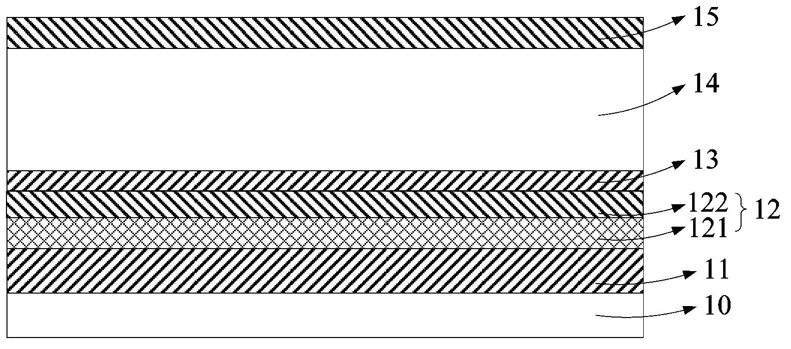
[0064] (1) Place the glass substrate on a 1×10 -4 In the vacuum coating chamber of Pa, a metal Ag film with a thickness of 200nm was prepared on the surface of the substrate by vacuum evaporation as a reflective electrode;

[0065] (2) Vacuum evaporation is used to evaporate a layer of CuPc film on the reflective electrode to obtain an active crystallization layer with a thickness of 20nm. The substrate temperature is 150°C and the evaporation rate is 1nm / s; Next, evaporate a layer of NPB film to obtain an induced crystallization layer with a thickness of 20nm and an evaporation rate of 1nm / s; after the preparation, cool to 25°C at a rate of 20°C / min;

[0066] (3) A layer of ITO film with a thickness of 100nm was sputtered on the surface of the crystalline organic layer by magnetron sputtering as the first transmission electrode;

[0067] (4) Prepare a light-emitting functio...

Embodiment 2

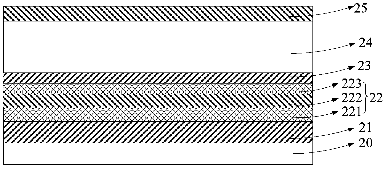
[0072] The difference between this embodiment and embodiment 1 is that the thickness of the NPB thin film of the induced crystallization layer is 40nm, and after the crystalline organic layer is prepared, it is cooled to 25°C at a rate of 10°C / min.

Embodiment 3

[0074] The difference between this embodiment and Example 1 is that the thickness of the active crystallization layer CuPc film is 30nm, the thickness of the induced crystallization layer NPB film is 30nm, and after the crystalline organic layer is prepared, it is cooled to 25°C at a rate of 5°C / min. ℃.


PUM


Abstract

The invention provides an organic light emission diode device. The organic light emission diode device comprises a substrate, and a reflection electrode, a crystallization organic layer, a first transmission electrode, a light emission function layer and a second transmission electrode which are sequentially laminated on the substrate, the material of the crystallization organic layer comprises an active crystallization material and an induction crystallization material, the active crystallization material is copper phthalocyanine, and the induction crystallization material is N,N'-diphenyl-N,N'-bis (3-methyl phenyl)-1,1'-biphenyl-4,4'-diamine or 4,7-bis (4-tri-aminoethyl)-2,1,3-diazosulfide. In the organic light emission diode device, through the arrangement of the crystallization organic layer formed by the active crystallization material and the induction crystallization material on the surface of the reflection electrode, the reflectivity of the device is greatly reduced, and the device has the characteristics of high contrast and excellent luminous efficiency. The invention also provides a fabrication method of the organic light emission diode device.

Description

technical field [0001] The invention relates to an organic electroluminescent device, in particular to an organic electroluminescent device and a preparation method thereof. Background technique [0002] Organic Light Emission Diode, hereinafter referred to as OLED, has the characteristics of high brightness, wide range of material selection, low driving voltage, fully cured active light emission, etc., and has the advantages of high definition, wide viewing angle, and fast response speed. It is a display technology and light source with great potential, which conforms to the development trend of mobile communication and information display in the information age, as well as the requirements of green lighting technology, and is the focus of many researchers at home and abroad. [0003] In the existing top-emitting OLED light-emitting device, light is generally reflected by the reflective electrode at the bottom, and then emitted from the transmissive electrode at the top. S...

Claims


Application Information

Patent Timeline
Patent Type & Authority Applications(China)
IPC IPC(8): H01L51/52H01L51/56
CPCH10K85/60H10K85/654H10K85/371H10K50/858H10K71/00
Inventor 周明杰冯小明黄辉王平
Owner OCEANS KING LIGHTING SCI&TECH CO LTD
Why Eureka
Try Eureka