Method for manufacturing thin film transistor and thin film transistor

A technology of thin-film transistors and polysilicon layers, which is applied in the manufacture of transistors, semiconductor devices, semiconductor/solid-state devices, etc., to achieve the effect of simplifying the manufacturing process and satisfying precise control

Active Publication Date: 2017-11-10
BOE TECH GRP CO LTD +1
View PDF4 Cites 0 Cited by
  • Summary
  • Abstract
  • Description
  • Claims
  • Application Information

AI Technical Summary

Problems solved by technology

[0014] However, there is no better solution in the prior art to better control the size of the LDD structure

Method used


Image

  • Method for manufacturing thin film transistor and thin film transistor
  • Method for manufacturing thin film transistor and thin film transistor
  • Method for manufacturing thin film transistor and thin film transistor

Examples


Embodiment Construction

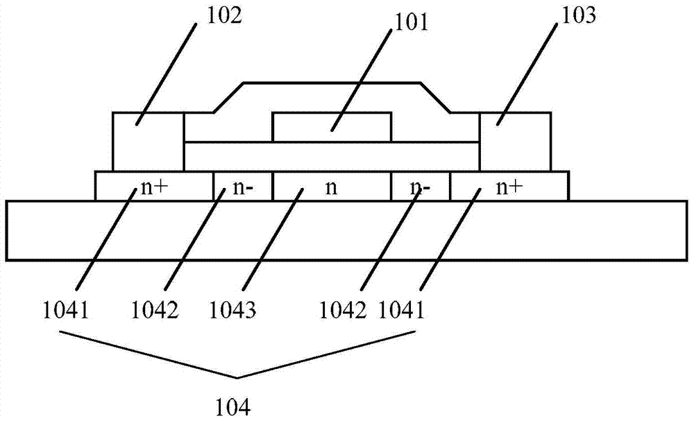
[0041] In the embodiment of the present invention, when forming the n+ region and n- region of the LTPS TFF, the above-mentioned n+ region and n- region are formed by using the photoresist defining the gate pattern and the gate target pattern as shields respectively. The resist precision and gate target pattern precision are controllable, so that the precision of the n-region can meet the precise control of the LDD structure size of the low-temperature polysilicon thin film transistor, and simplify the manufacturing process of the LTPS TFF.

[0042] Before the method of the embodiment of the present invention is described in detail, several process flows involved in the embodiment of the present invention are briefly described, so as to better understand the embodiment of the present invention.

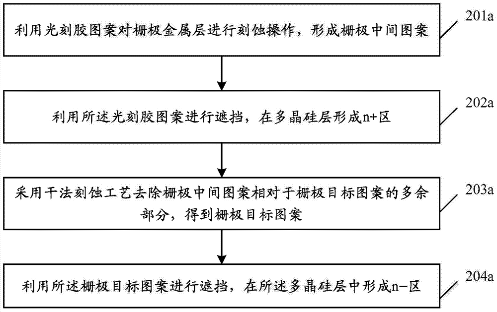
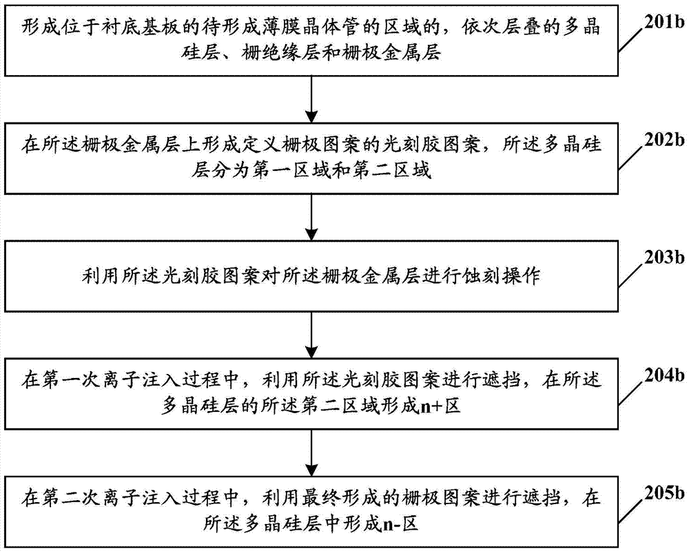
[0043] In semiconductor manufacturing, it is necessary to use selected images, graphics or objects to block the film layer to be processed in order to control the active area of ​​etch...


PUM


Abstract

A low-temperature poly-silicon thin film transistor and a manufacturing method therefor. The method comprises: carrying out an etching operation on a gate metal layer by using a photoresist pattern (105) to form a gate intermediate pattern (106), the size of the gate intermediate pattern (106) being greater than the size of a gate target pattern (101); carrying out shielding by using the photoresist pattern (105), and forming an n+ region (1041) in a poly-silicon layer (104); removing a redundant part, relative to the gate target pattern (101), of the gate intermediate pattern (106) by using a dry etching technology, so as to obtain the gate target pattern (101); and carrying out shielding by using the gate target pattern (101), and forming an n- region (1042) in the poly-silicon layer. The precision of the n- region of the manufactured thin film transistor can meet requirements for accurate control of the low-temperature poly-silicon thin film transistor over the size of an LDD structure, and the manufacturing technological process of the LTPS TFF is simplified.

Description

technical field [0001] The invention relates to a thin-film transistor, in particular to a method for manufacturing a low-temperature polysilicon thin-film transistor and the low-temperature polysilicon thin-film transistor. Background technique [0002] Thin Film Transistor Liquid Crystal Display (TFTLD) can be divided into polysilicon and amorphous silicon, the difference between the two lies in the characteristics of the transistor. The molecular structure of polysilicon is arranged in a neat and directional manner in a crystal grain, so the electron mobility of polysilicon is higher than that of disordered amorphous silicon, so it has been widely used. [0003] Polysilicon mainly includes high-temperature polysilicon and low-temperature polysilicon. [0004] TFTs made of low-temperature polysilicon are divided into two types: N-type and P-type. N-type low-temperature polysilicon TFTs need to be provided with a low-doped drain (Lightly Drain Doping, LDD) to reduce the le...

Claims


Application Information

Patent Timeline
Patent Type & Authority Patents(China)
IPC IPC(8): H01L21/336H01L29/786
CPCH01L29/66757H01L29/78621H01L29/78675H01L29/786
Inventor 李淳东刘华锋李知勋
Owner BOE TECH GRP CO LTD
Why Eureka
Try Eureka