Electrostatic protection circuit

An electrostatic protection and circuit technology, applied in the direction of emergency protection circuit devices, circuits, circuit devices, etc., can solve the problems of MOS transistor malfunction and poor internal circuit operation.

Inactive Publication Date: 2014-12-24
KK TOSHIBA
View PDF4 Cites 3 Cited by
  • Summary
  • Abstract
  • Description
  • Claims
  • Application Information

AI Technical Summary

Problems solved by technology

However, the RCTMOS circuit also responds to the fluctuation of the power supply voltage due to the operation of the internal circuit, and the MOS transistor for discharge may malfunction
Due to the malfunction of the MOS transistor for discharge, the power supply voltage drops and the malfunction of the internal circuit occurs.

Method used


Image

  • Electrostatic protection circuit
  • Electrostatic protection circuit
  • Electrostatic protection circuit

Examples


no. 1 approach )

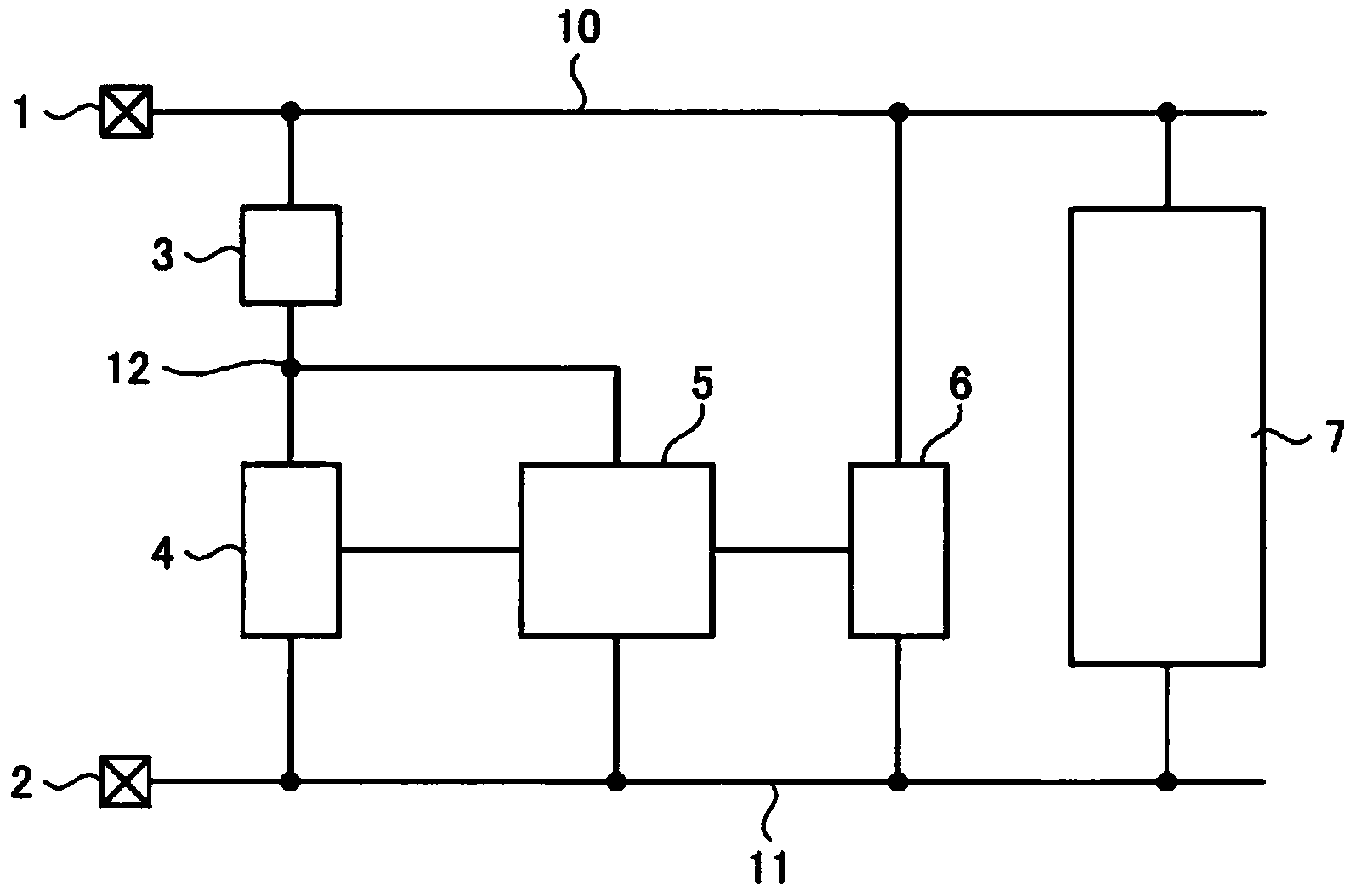
[0028] figure 1 It is a figure which shows the electrostatic protection circuit of 1st Embodiment. The electrostatic protection circuit of this embodiment has a clamp circuit 3 , a trigger circuit 4 , a snubber circuit 5 and a switch circuit 6 . The first power supply line 10 is connected to the first power supply terminal 1 , and applies, for example, a predetermined power supply voltage VCC to the first power supply terminal 1 to which a high potential side power supply voltage is applied. The second power supply line 11 is connected to the second power supply terminal 2 and is supplied with a low potential side power supply voltage. For example, a ground potential is applied to the second power supply terminal 2 as a low potential side power supply voltage. A clamping circuit 3 is connected between the first power line 10 and the first connection point 12 . For example, when a positive ESD surge is applied to the first power supply terminal 1 relative to the second power...

no. 2 approach )

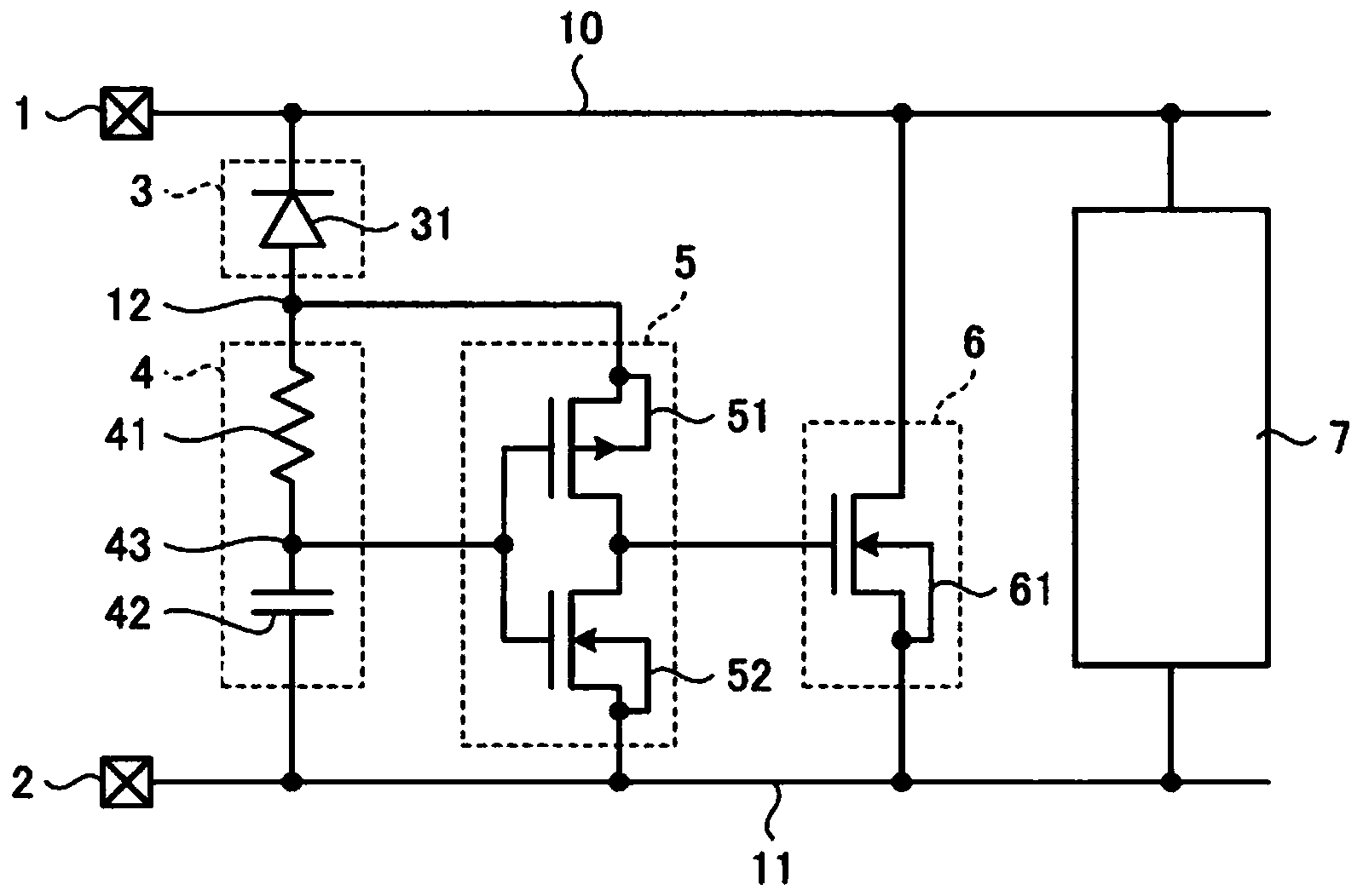
[0032] figure 2 It is a figure which shows the electrostatic protection circuit of 2nd Embodiment. Components corresponding to those of the first embodiment are assigned the same reference numerals, and description thereof will be omitted. In the present embodiment, the clamp circuit 3 has a diode 31 that is reverse-biased by the power supply voltage applied to the first power supply line 10 and the second power supply line 11 . The trigger circuit 4 connected between the first power line 10 and the first connection point 12 has a series circuit of a resistor 41 and a capacitor 42 . The common connection point 43 of the resistor 41 and the capacitor 42 becomes the output terminal of the trigger circuit 4 .

[0033] The buffer circuit 5 biased by the voltage between the first connection point 12 and the second power supply line 11 has a CMOS converter composed of a PMOS transistor 51 and an NMOS transistor 52 . The gate electrodes of the PMOS transistor 51 and the NMOS tran...

no. 3 approach )

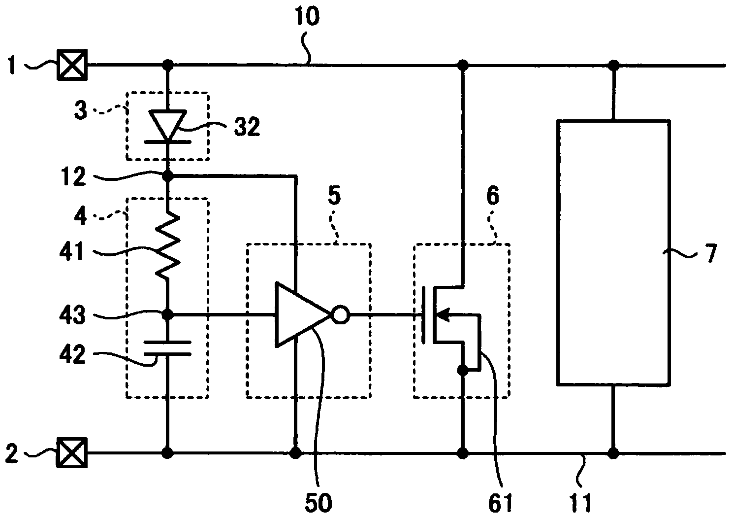
[0041] image 3 It is a figure which shows the electrostatic protection circuit of 3rd Embodiment. Components corresponding to the above-described embodiments are given the same reference numerals, and explanations thereof are omitted. In the electrostatic protection circuit of the present embodiment, the clamp circuit 3 connected between the first power line 10 and the first connection point 12 has the function of controlling the power supply voltage applied between the first power line 10 and the second power line 11. forward biased diode 32 . The common connection point 43 constituting the output terminal of the flip-flop circuit 4 is connected to the input terminal of the converter 50 constituting the buffer circuit 5 . The converter 50 is biased by the voltage between the first connection point 12 and the second power supply line 11 .

[0042] In a stable bias state where a predetermined power supply voltage is applied between the first power supply terminal 1 and the ...


PUM


Abstract

An object of the invention to provide an electrostatic protection circuit for suppressing a malfunction of the swing of the power supply voltage. The electrostatic protection circuit includes a first high-potential side power supply line (10), a second low-potential side power supply line (11) and a first connection point (12). Between the first power supply line (10) and the first connection point (12), a clamp circuit (3) is connected, in which a current is dramatically increased when flowing through a predetermined threshold voltage. Between the first connection point (12) and the second power supply line (11), a trigger circuit (4) is connected, which responds to the current change of the clamp circuit (3) and outputs a trigger signal. A buffer circuit (5), in which the voltage is biased when passing across the voltage between the first connection point (12) and the second power supply line (11), responds to the trigger signal of the trigger circuit (4) and outputs a drive signal. A switching circuit (6) which is turned on / off corresponding to the drive signal of the the buffer circuit (5) is connected between the first power supply line (10) and the second power supply line (11).

Description

technical field [0001] Embodiments of the present invention relate to electrostatic protection circuits. Background technique [0002] Conventionally, various protection circuits against electrostatic discharge (ESD: Electrostatic Discharge) have been proposed. The so-called ESD is electrostatic discharge, and refers to the discharge of a semiconductor device from a person or machine charged by static electricity, or the discharge of a charged semiconductor device to a ground potential. For semiconductor devices, when ESD discharge occurs, a large amount of charge flows into the semiconductor device from its terminals, and this charge generates a high voltage inside the semiconductor device, causing insulation breakdown of internal components and failure of the semiconductor device. For this reason, an electrostatic protection circuit is a necessary technology for semiconductor integrated circuits. [0003] Typical examples of electrostatic protection circuits include RCT ...

Claims


Application Information

Patent Timeline
Patent Type & Authority Applications(China)
IPC IPC(8): H01L27/02
CPCH02H9/046
Inventor 一岐村岳人
Owner KK TOSHIBA
Why Eureka
Try Eureka