Transparent conductive substrate fabrication method, transparent conductive substrate and electrostatic capacitance-type touch panel
A transparent conductive and transparent substrate technology, applied in transparent dielectrics, printed circuit manufacturing, cable/conductor manufacturing, etc., which can solve problems such as disappearance of conductivity, pattern collapse, and inability to ensure patterns.
- Summary
- Abstract
- Description
- Claims
- Application Information
AI Technical Summary
Problems solved by technology
Method used
Image

Examples
no. 1 Embodiment approach
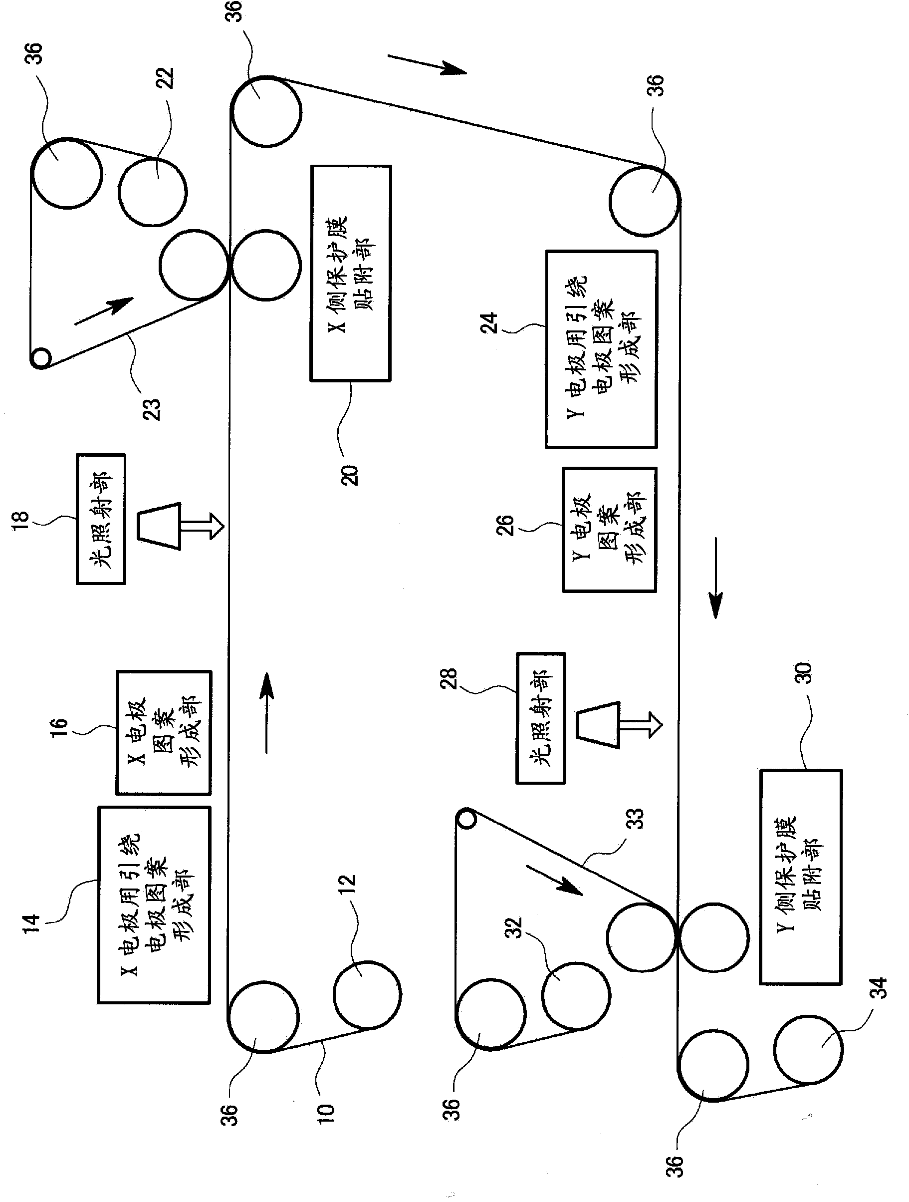
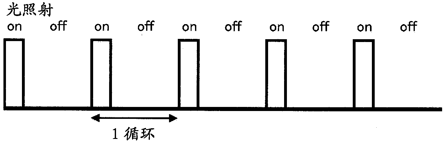
[0045] figure 1 An example of a manufacturing process of the transparent conductive substrate for a capacitive touch panel according to the embodiment is shown. exist figure 1 In this process, while pulling out the transparent substrate (transparent film substrate) 10 from the substrate roll 12, the X electrode (corresponding to the first electrode) is used to form the X electrode (corresponding to the first electrode) on one main surface of the transparent film substrate 10 with the lead electrode pattern forming part 14. The electrode uses a lead electrode pattern. The routing electrode pattern for the X electrode is, for example, Figure 9 pattern shown. The X electrode lead electrode pattern forming unit 14 forms a X electrode lead electrode pattern by a printing method such as screen printing, gravure printing, or flexo printing using a known conductive paste, and then dries it. Here, as a drying method, heating by an oven, heating by pulse light irradiation, etc. ar...
no. 2 Embodiment approach
[0088] Figure 5 Another example of the manufacturing process of the transparent conductive substrate for the capacitive touch panel according to the embodiment is shown in figure 1 The same elements are marked with the same reference numerals. exist Figure 5 In this example, while pulling out the first transparent film substrate 10a from the first substrate roll 12a, the lead electrode pattern forming part 14 for the X electrode (corresponding to the first electrode) is placed on one main part of the first transparent film substrate 10a. Form the lead electrode pattern for the X electrode on the surface, and dry it.
[0089] On the main surface of the first transparent film substrate 10 a on which the X electrode routing electrode pattern is formed, the X electrode pattern forming unit 16 forms an X electrode pattern using the transparent conductive pattern forming ink. This X-electrode pattern is formed so as to be connected to the aforementioned X-electrode routing ele...
Embodiment 1
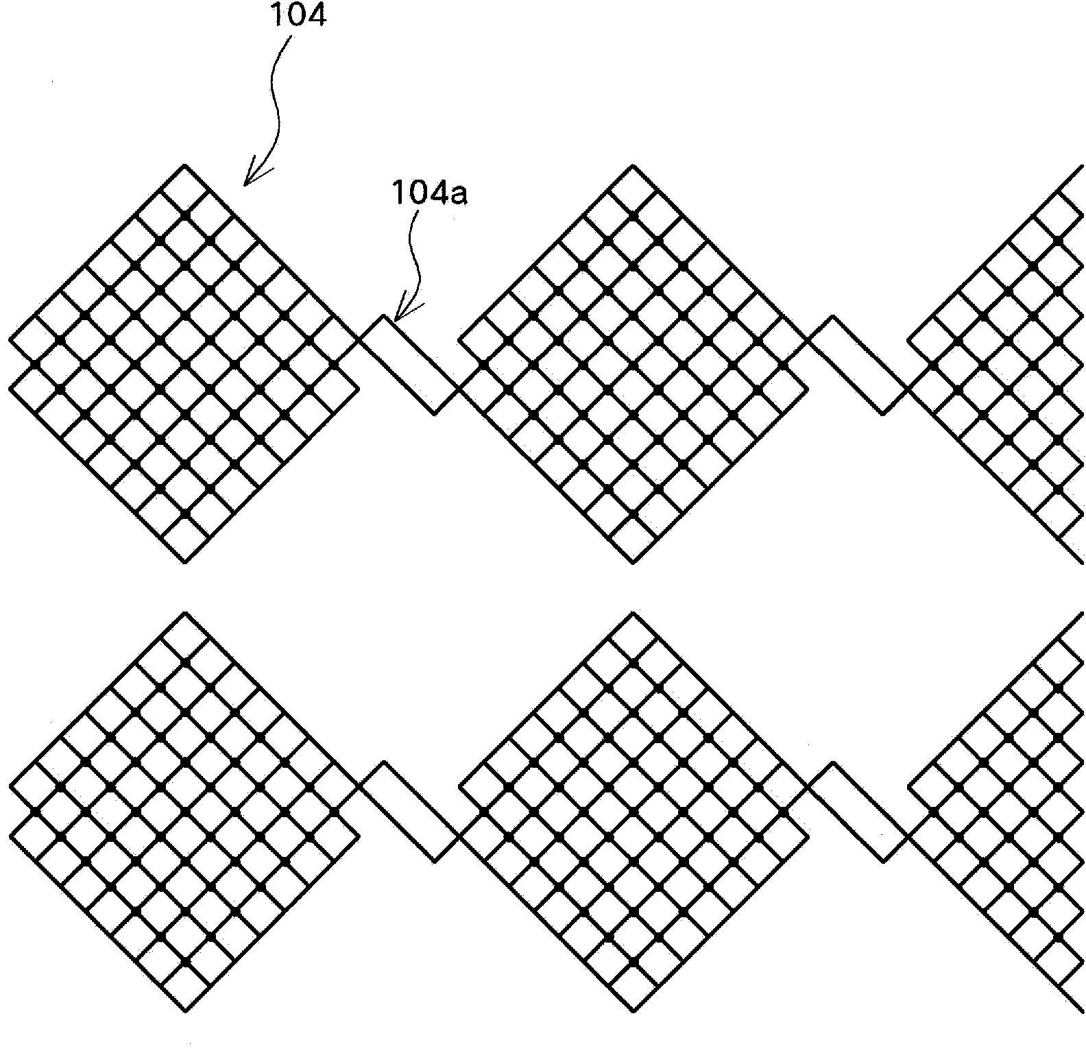
[0112] Make the following sequence with Figure 7 , Figure 8 The patterns shown are transparent conductive substrates. in addition, Figure 7 The pattern is as follows: 25 rhombuses (obtained by tilting the square at 45°C) are connected in a row along the horizontal direction of the figure in the connection area, and triangles obtained by removing half of the rhombus are connected at both ends of the row. 45 rows are arranged in the vertical direction of the figure, and the upper and lower rows are not electrically connected. in addition, Figure 8 The pattern is as follows: 45 rhombuses are connected in a column along the vertical (up and down) direction of the figure in the connection area, and at one end of the column (in Figure 8 The lower end in the center) is connected to the triangle obtained by removing half of the rhombus, and such columns are arranged in 25 columns along the horizontal direction of the figure, and the left and right columns are not electrically...
PUM
| Property | Measurement | Unit |
|---|---|---|
| viscosity | aaaaa | aaaaa |
| particle diameter | aaaaa | aaaaa |
| electrical resistance | aaaaa | aaaaa |
Abstract
Description
Claims
Application Information
 - R&D
- Intellectual Property
- Life Sciences
- Materials
- Tech Scout
- Unparalleled Data Quality
- Higher Quality Content
- 60% Fewer Hallucinations
Browse by: Latest US Patents, China's latest patents, Technical Efficacy Thesaurus, Application Domain, Technology Topic, Popular Technical Reports.
© 2025 PatSnap. All rights reserved.Legal|Privacy policy|Modern Slavery Act Transparency Statement|Sitemap|About US| Contact US: help@patsnap.com