White organic light-emitting device and preparation method thereof

An electroluminescence and white technology, which is applied in the field of white organic electroluminescence devices and their preparation, and can solve the problems of low color recovery coefficient and insufficient coverage.

Active Publication Date: 2015-01-07
CHANGCHUN INST OF APPLIED CHEMISTRY - CHINESE ACAD OF SCI
View PDF4 Cites 3 Cited by
  • Summary
  • Abstract
  • Description
  • Claims
  • Application Information

AI Technical Summary

Problems solved by technology

The device has high luminous efficiency, but the characteristics of double-peak emission lead to insuffic...

Method used


Image

  • White organic light-emitting device and preparation method thereof
  • White organic light-emitting device and preparation method thereof
  • White organic light-emitting device and preparation method thereof

Examples


preparation example Construction

[0076] The present invention also provides a method for preparing a white organic light-emitting device described in the above technical solution, comprising the following steps:

[0077] providing an anode layer on the substrate;

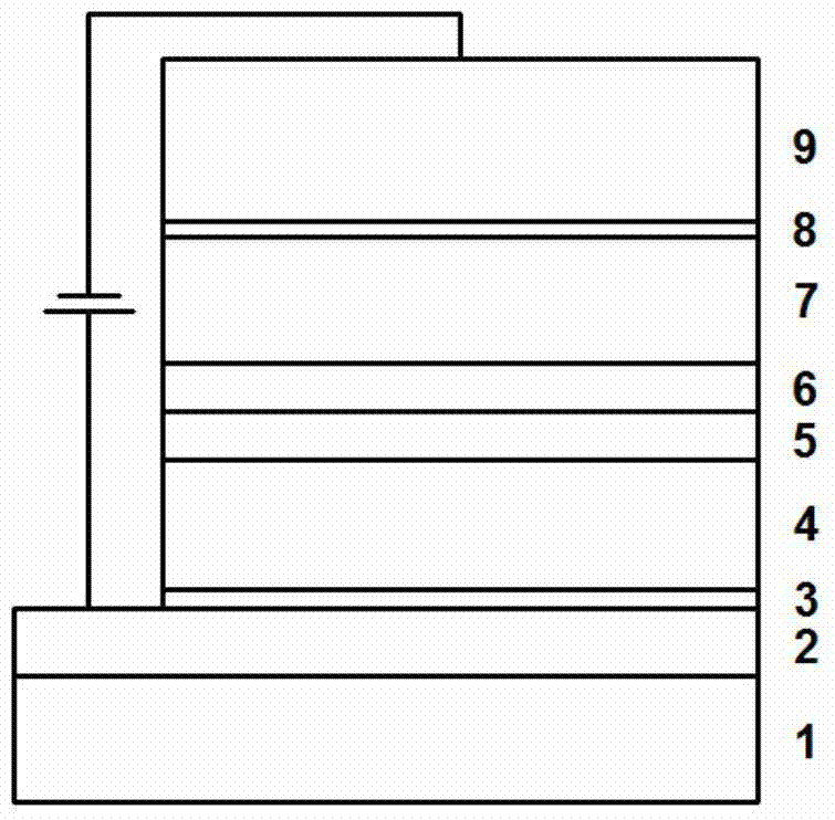
[0078] On the surface of the anode layer, an anode modification layer, a hole transport-electron blocking layer, a hole-dominated light-emitting layer, an electron-dominated light-emitting layer, a hole block-electron transport layer, a cathode modification layer and a cathode layer are sequentially evaporated to obtain a white organic Light emitting devices.

[0079] The invention provides a substrate on which an anode layer is arranged. In the present invention, the substrate is consistent with the substrate described in the above technical solution, and will not be repeated here. In the present invention, the anode material provided on the substrate is preferably etched to form a strip electrode on the substrate, and an anode layer is obtained...

Embodiment 1

[0097] First, the ITO anode layer on the ITO glass is laser-etched into a strip electrode, and then ultrasonically cleaned with cleaning solution and deionized water for 15 minutes and dried in an oven; then the dried substrate is placed in a pre-treatment vacuum Chamber, under the atmosphere with a vacuum degree of 10Pa, the ITO anode is subjected to low-pressure plasma treatment with a voltage of 400 volts for 3 minutes, and then transferred to the organic evaporation chamber;

[0098] In a vacuum of 1×10 -5 Pa~2×10 -5 In the organic evaporation chamber of Pa, 3nm thick MoO was sequentially evaporated on the ITO layer at a rate of 0.01nm / s 3 Anode modification layer 3; TAPC hole transport-electron blocking layer 4 with a thickness of 40nm was evaporated at a rate of 0.05nm / s; PQ was evaporated at a rate of 0.0013nm / s 2 Ir (dpm), 0.0035nm / s rate evaporation Ir (ppy) and 0.05nm / s rate evaporation TcTa obtain 5nm thick hole-dominated light-emitting layer 5; with 0.0001nm / s ra...

Embodiment 2

[0106] First, the ITO anode layer on the ITO glass is laser-etched into strip electrodes, and then ultrasonically cleaned with cleaning solution and deionized water for 15 minutes and dried in an oven. Then put the dried substrate into the pretreatment vacuum chamber, and then transfer the ITO anode to the organic evaporation chamber after a 3-minute low-pressure plasma treatment with a voltage of 400 volts in an atmosphere with a vacuum degree of 10 Pa;

[0107] In a vacuum of 1×10 -5 Pa~2×10 -5 In the organic evaporation chamber of Pa, 3nm thick MoO was sequentially evaporated on the ITO layer at a rate of 0.01nm / s 3 Anode modification layer 3; TAPC hole transport-electron blocking layer 4 with a thickness of 40nm was evaporated at a rate of 0.05nm / s; PQ was evaporated at a rate of 0.0012nm / s 2 Ir(dpm), 0.003nm / s rate evaporation Ir(ppy) 3 Evaporating mCP at a rate of 0.05nm / s and 0.05nm / s to obtain a 5nm-thick hole-dominated light-emitting layer 5; CzSi obtains a 10nm-t...


PUM

PropertyMeasurementUnit
Thicknessaaaaaaaaaa
Thicknessaaaaaaaaaa
Thicknessaaaaaaaaaa

Abstract

The invention provides a white organic light-emitting device. The white organic light-emitting device is formed by sequential arrangement of a substrate, an anode layer, an anode modification layer, a hole transport-electron barrier layer, a hole leading light-emitting layer, an electron leading light-emitting layer, a hole barrier-electron transport layer, a cathode modification layer and a cathode layer, wherein the electron leading light-emitting layer comprises the following components in percentage by weight: 0.05-2.0 percent of organic sensitized materials, 8.0-25.0 percent of blue organic light-emitting materials and the balance of electron-type organic main body materials; the organic sensitized materials are transition metal complexes of which the energy level and the energy are matched. According to the white organic light-emitting device, the organic sensitized materials are doped into the electron leading light-emitting layer and function as a deep current carrier constraint center and an energy transfer ladder, so that a light-emitting interval is expanded, the transfer of the energy from the main body material to the light-emitting material is accelerated, and therefore, the white organic light-emitting device provided by the invention has higher efficiency and higher color recovery coefficient.

Description

technical field [0001] The invention relates to the technical field of electroluminescence, in particular to a white organic electroluminescence device and a preparation method thereof. Background technique [0002] An organic electroluminescent device is a self-luminous device that generates light when charges are injected into an organic film between a hole injection electrode (anode) and an electron injection electrode (cathode), and the electrons and holes combine and then annihilate . Organic electroluminescent devices have the characteristics of low voltage, high brightness, wide viewing angle, etc., so organic electroluminescent devices have been developed rapidly in recent years. Among them, white organic electroluminescent devices have become a research hotspot due to their application prospects in full-color display and solid-state lighting. [0003] For a long time, trivalent iridium complexes have been regarded as ideal organic electroluminescent materials by a...

Claims


Application Information

Patent Timeline
IPC IPC(8): H01L51/50H01L51/54H01L51/56
CPCH10K85/146H10K85/342H10K50/121H10K50/80H10K50/00H10K71/00
Inventor 周亮张洪杰李成宇
Owner CHANGCHUN INST OF APPLIED CHEMISTRY - CHINESE ACAD OF SCI
Why Eureka
Try Eureka