Back structure protecting method

A backside structure and backside technology, applied in electrical components, semiconductor/solid-state device manufacturing, circuits, etc., can solve the problems of device parameter degradation, product failure, pattern change, etc., and achieve the effect of simple process, high control precision, and easy implementation.

Active Publication Date: 2015-01-14
CSMC TECH FAB2 CO LTD
View PDF5 Cites 3 Cited by
  • Summary
  • Abstract
  • Description
  • Claims
  • Application Information

AI Technical Summary

Problems solved by technology

[0002] At present, in the manufacturing process of semiconductor devices, it is necessary to perform ion implantation and well pushing process on the wafer. Usually, the well pushing time is long and the temperature is high. Therefore, for some semiconductor devices with back structure, during the well pushing process, The pattern or implanted area on the back of the wafer is easily affected by other steps in the process: on the one hand, whe

Method used


Image

  • Back structure protecting method
  • Back structure protecting method
  • Back structure protecting method

Examples


Embodiment Construction

[0024] In order to make the above objects, features and advantages of the present invention more comprehensible, the present invention will be further described in detail below in conjunction with the accompanying drawings and specific embodiments.

[0025] Reference herein to "one embodiment" or "an embodiment" refers to a particular feature, structure or characteristic that can be included in at least one implementation of the present invention. "In one embodiment" appearing in different places in this specification does not all refer to the same embodiment, nor is it a separate or selective embodiment that is mutually exclusive with other embodiments.

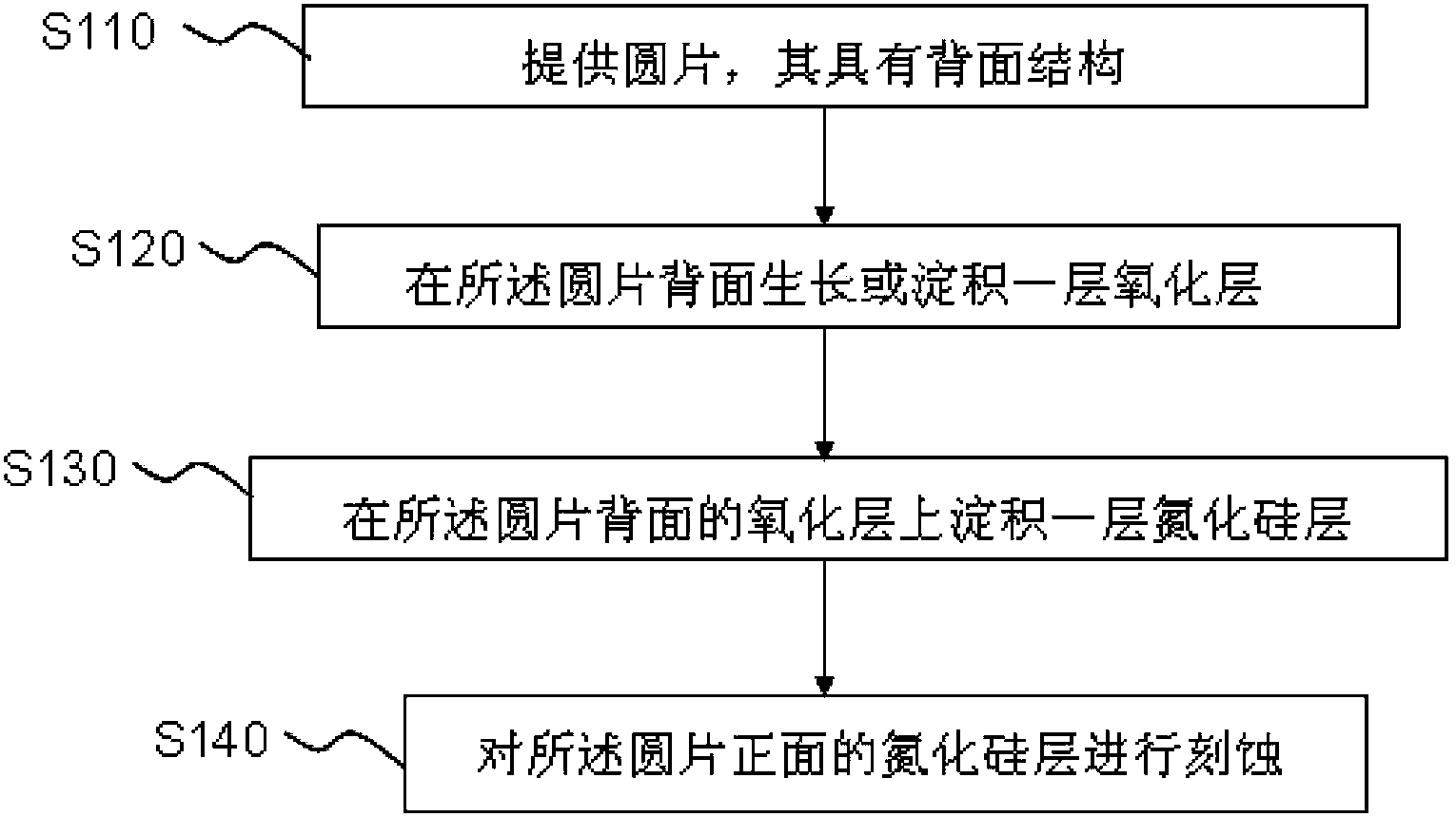
[0026] see figure 1 , which is a flowchart of the method of the present invention. Such as figure 1 As shown, the protection method of a kind of back structure of the present invention, its concrete steps are as follows:

[0027] Step 1 S110: providing a semiconductor wafer having a backside structure. Wherein, the manuf...


PUM

PropertyMeasurementUnit
Thicknessaaaaaaaaaa
Thicknessaaaaaaaaaa
Thicknessaaaaaaaaaa

Abstract

The invention provides a back structure protecting method. The method is about growing a protective layer on the back side of a wafer to protect the back structure of the wafer. The method comprises the steps of providing a wafer which is provided with a back structure, growing or depositing an oxide layer on the back side of the wafer, depositing a silicon nitride layer on the oxide layer on the back side of the wafer, and conducting subsequent technological fabrication. Compared with the prior art, the method has the advantage that the purpose of protecting the back side of the wafer is realized by growing the protective layer on the back side of the wafer, the silicon nitride layer serves as the outmost protective layer, and the back structure of the wafer is prevented from being affected by other technological processes by means of the fact that impurities are low in diffusivity and not prone to oxidation in silicon nitride. The method is easy to implement and high in control precision, the technology is simple, and the back structure of the wafer can be well protected without affecting the front side.

Description

technical field [0001] The invention relates to the field of semiconductor manufacturing, in particular to a method for protecting a back structure. Background technique [0002] At present, in the manufacturing process of semiconductor devices, it is necessary to perform ion implantation and well pushing process on the wafer. Usually, the well pushing time is long and the temperature is high. Therefore, for some semiconductor devices with back structure, during the well pushing process, The pattern or implanted area on the back of the wafer is easily affected by other steps in the process: on the one hand, when the wafer is in the push-well furnace, the impurities in the push-well furnace tube itself will re-dope the back of the wafer, making the original back-side injection Changes in concentration or junction depth will eventually lead to device parameter degradation or failure; moreover, oxidation will also cause changes in the concentration on the back surface of the wa...

Claims


Application Information

Patent Timeline
IPC IPC(8): H01L21/314
CPCH01L21/02016H01L21/02164H01L21/0217
Inventor 芮强张硕王根毅邓小社
Owner CSMC TECH FAB2 CO LTD
Why Eureka
Try Eureka