GaN-based green light LED structure with p type buffering layer and growing method of GaN-based green light LED structure

A buffer layer and p-type technology, applied in the field of optoelectronics, can solve the problems of poor antistatic ability and damage, and achieve the effects of reducing breakdown rate, improving luminous efficiency, and realizing temperature gradient

Active Publication Date: 2015-01-14
华芯半导体科技有限公司
View PDF5 Cites 3 Cited by
  • Summary
  • Abstract
  • Description
  • Claims
  • Application Information

AI Technical Summary

Problems solved by technology

In the traditional epitaxial growth process, the high-temperature p-type GaN layer is usually directly grown after the growth of the low-temperature multiple quantum well material. Due to the large difference in growth temperature in this epitaxial process, it is easy to cause damage to the InGaN quantum wells of adjacent periods, making the InGaN material The In group is analyzed, resulting in poor antistatic ability

Method used


Image

  • GaN-based green light LED structure with p type buffering layer and growing method of GaN-based green light LED structure

Examples


Embodiment Construction

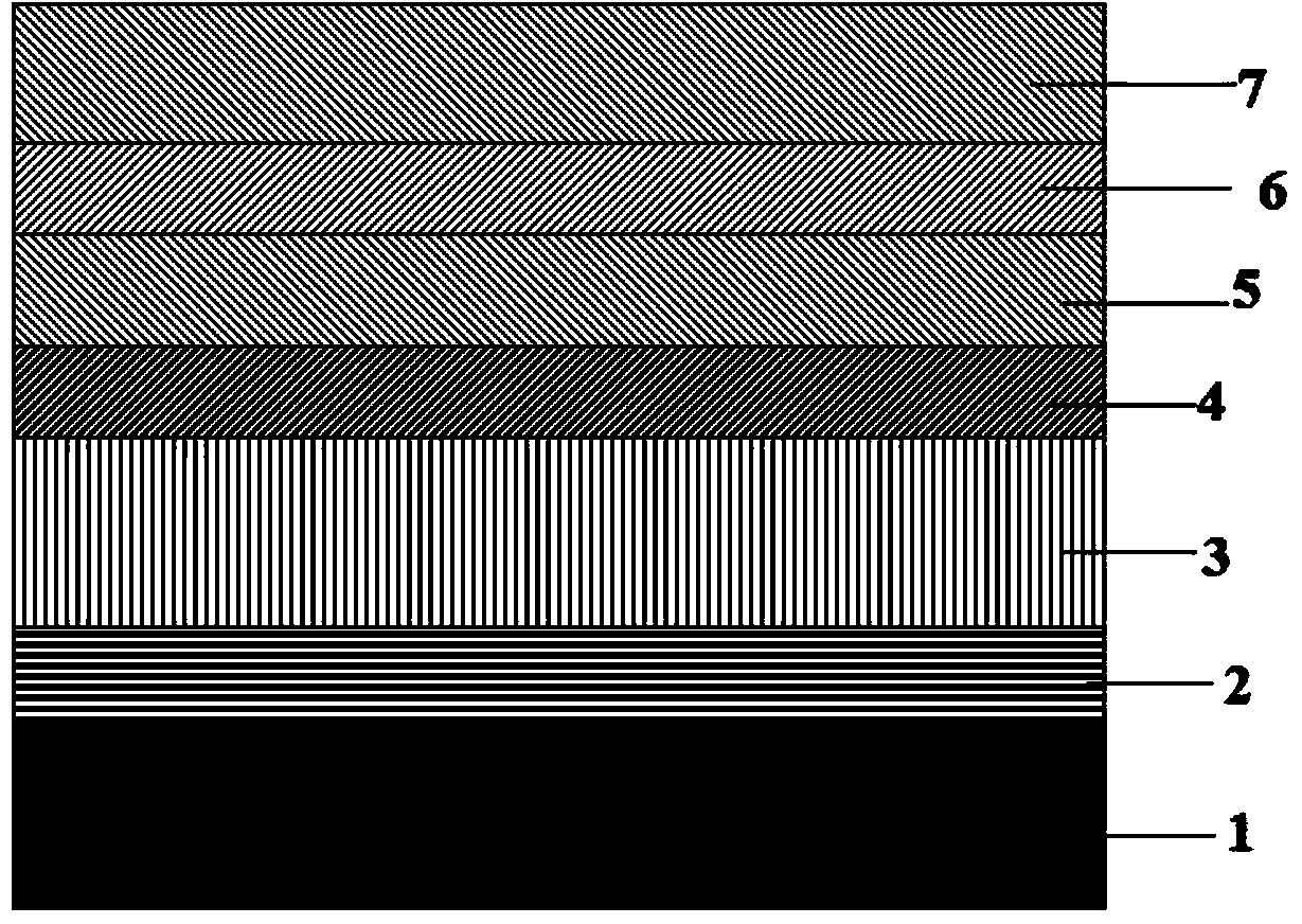
[0012] Such as figure 1 As shown, a GaN-based LED green light structure with a p-type buffer layer, a GaN nucleation layer 2, an undoped GaN layer 3, an n-type GaN layer 4, and a low-temperature In x Ga 1-x N / GaN multi-quantum well layer 5 , p-type buffer layer 6 , and high-temperature p-type GaN layer 7 .

[0013] A GaN-based LED green light structure with a p-type buffer layer, which sequentially includes a sapphire substrate layer 1, a GaN nucleation layer 2, an undoped GaN layer 3, an n-type GaN layer 4, and a low-temperature In x Ga 1-x N / GaN multi-quantum well layer 5 and high-temperature p-type GaN layer 6 are characterized by low-temperature In x Ga 1-x A p-type buffer layer 6 is grown between the N / GaN multi-quantum well layer 5 and the high-temperature p-type GaN layer 7 .

[0014] The p-type buffer layer 6 is composed of multiple layers of p-type In with different In compositions. y Ga 1-y Composed of thin N layers, the multilayer In y Ga 1-y N thin layers ...


PUM


Abstract

The invention discloses a GaN-based green light LED structure with a p type buffering layer and a growing method of the GaN-based green light LED structure. The GaN-based green light LED structure comprises a sapphire substrate layer, a GaN nucleating layer, a non-doping GaN layer, an n type GaN layer, a low-temperature InxGa1-xN/GaN multiple quantum well layer and a high-temperature p type GaN layer from bottom to top in sequence. The GaN-based green light LED structure is characterized in that the p type buffering layer grows between the low-temperature InxGa1-xN/GaN multiple quantum well layer and the high-temperature p type GaN layer. The p type buffering layer is composed of a plurality of p type InyGa1-yN thin layers with gradually changing components, and the growing temperature gradually increases from bottom to top. Compared with a traditional epitaxial structure, the gradual temperature changing can be effectively achieved, the damage to a low-temperature InGaN quantum well structure when the high-temperature p type GaN layer grows is lowered, the antistatic ability of an epitaxial wafer is improved, and therefore the breakdown rate of a chip is reduced, and the light emitting efficiency of the chip is improved.

Description

technical field [0001] The invention relates to the technical field of optoelectronics, in particular to a GaN-based green LED structure and a growth method thereof. Background technique [0002] At present, more and more green LED-related products have begun to appear on the market. Green LEDs have a wide range of applications and can be applied to large indoor and outdoor display screens, traffic lights, backlights (tablet PCs, mobile phone displays, etc.), portable lighting system, fixed color lighting system, optical storage system and many other fields. The market share of green LED-related products is also gradually increasing, and the market has higher and higher performance requirements for green LED products. How to obtain high-height, high-quality green LED products has become a research hotspot. [0003] However, since the In composition (20%--35%) in the quantum well InGaN material in the green LED epitaxial growth process is much higher than that in the blue L...

Claims


Application Information

Patent Timeline
Patent Type & Authority Applications(China)
IPC IPC(8): H01L33/12H01L33/00
CPCH01L33/005H01L33/0066H01L33/12H01L2933/0008
Inventor 王智勇张杨杨翠柏杨光辉
Owner 华芯半导体科技有限公司
Why Eureka
Try Eureka